Mounting structure of electronic component

a technology of electronic components and mounting structures, applied in the direction of optics, instruments, printed circuit aspects, etc., can solve the problems of insufficient bonding strength, fluctuation in distance, contact defects, etc., to improve the reliability of conductive connection status, improve bonding strength, and improve the effect of bonding strength

Active Publication Date: 2012-01-31
SEIKO EPSON CORP
View PDF11 Cites 2 Cited by
  • Summary
  • Abstract
  • Description
  • Claims
  • Application Information

AI Technical Summary

Benefits of technology

[0012]An advantage of the invention is to provide a mounting structure of an electronic component that exhibits an improved bonding strength between a bump electrode and a terminal on a substrate with improved reliability in a conductive connection status.
[0013]According to an aspect of the invention, a mounting structure of an electronic component includes: a bump electrode included in the electronic component, the bump electrode having an internal resin as a core and a conductive film covering a surface of the internal resin, and elastically deforming so as to follow a shape of at least one corner of a terminal so that the conductive film makes direct conductive contact with at least part of a top surface of the terminal and at least part of a surface along a thickness direction of the terminal; a substrate having the terminal and the electronic component that is mounted on the substrate; and a holding unit provided to the substrate and the electronic component so as to hold a state in which the bump electrode electrically deformed makes conductive contact with the terminal.
[0014]According to this mounting structure of an electronic component, the bump electrode has the internal resin as a core. Therefore, by applying pressure on the terminal on the substrate, the bump electrode is easily pressed and reaches an elastically (compressively) deformed state. Bonding the bump electrode to the terminal with the aforementioned elastic deformation allows the bump electrode to follow the shape of the terminal, in order for the conductive film to be in directly conductive contact with at least part of the top surface as well as at least part of the surface along the thickness direction of the terminal, even is there is, for instance, a misalignment between the bump electrode and the terminal, causing the bump electrode to abut the corner of the terminal. Therefore, this conductive contact status being held with the holding unit ensures a sufficient contact area between the terminal and the conductive film of the bump electrode, and this provides a preferable conductive connection status.
[0015]Elastic restoring force (repelling force) increases the bonding strength between the internal resin and the terminal, the elastic restoring force being generated in the bump electrode against the terminal of the substrate due to the elastic deformation of the internal resin in the bump electrode, thereby improving the reliability of the conductive connection status. Specifically, the restoring force of the internal resin caused by the elastic deformation of the bump electrode works so that the bump electrode wraps the corner, the restoring force originating from following at least one corner shape of the terminal. Therefore, the bonding strength between the bump electrode and the terminal is increased as described.
[0016]It is preferable that, in the mounting structure of an electronic component, the holding unit be composed by a sealing resin filled and cured around a conductive contact area of the bump electrode and the terminal.
[0017]This ensures the more preferable status of conductive contact between the terminal and the elastically deforming bump electrode, thereby improving the conductive connection status between the terminal and the conductive film of the bump electrode.

Problems solved by technology

However, since lands and bump electrodes are generally formed with metal, a mispositioning during bonding and a misalignment caused by a low aligning precision of lands and bump electrodes may result in a contact defect (conductive defect) originating from insufficient bonding strength between these lands and bump electrodes.
Moreover, a fluctuation in distance may be caused between lands and bump electrodes by a warping of electronic components such as substrates and ICs as well as by a fluctuation in the height of lands and bump electrodes being formed.
This may result in an inability to obtain sufficient bonding strength between the bump electrodes and the terminals, causing a contact defect (conductive defect).
However, while the slipping, the sliding, and the inclination of connecting electrodes (bump electrode) arranged over the metal conductive layer are prevented by the anchor effect originating from the concavities and convexities of the metal conductive surface, the above-mentioned print circuit board does not have a structure that increases the bonding strength between the metal conductive substrate and the connecting electrode.
Further, the structure does not increase the bonding strength between a plurality of electrodes.
Consequently, occurrences of the mispositioning during bonding and the misalignment between electrodes (lands and bump electrodes) caused by low aligning precision therebetween may still result in a contact defect (conductive defect) originating from insufficient bonding strength between these electrodes.
This means that, if the distance between the lands and the electrodes are not constant as described above, the connecting electrodes may have a low capability in absorbing the distance deviation with elastic deformation, and therefore the bonding strength between these electrodes may be insufficient.
For this reason, the contact defect (conductive defect) may still occur as well.
In case of the pluralities of the terminals and the bump electrodes respectively being formed on the substrate and on the electronic component, a substrate distortion may cause a fluctuation in the height (level) of the bonding surface of each of the terminals.
Moreover, when coupling the substrate and the electronic component at the pluralities of bump electrodes and terminals, if there is a fluctuation in the distance between the bump electrodes and the terminals prior to their bonding, it becomes difficult to couple all the bump electrodes and all the terminals in a preferable strength.

Method used


Image

  • Mounting structure of electronic component
  • Mounting structure of electronic component
  • Mounting structure of electronic component

Examples


first embodiment

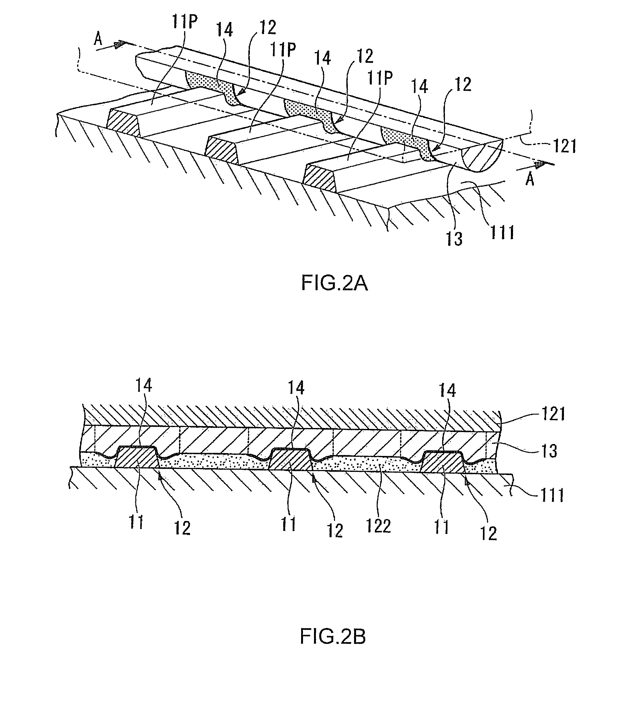
[0065]FIG. 4A is a drawing illustrating a status before mounting the electronic component 121 to the substrate 111, and is a magnified sectional view corresponding to the main parts of the FIG. 2B. Hereafter, the terminals 11, the bump electrodes 12, and the conductive films 14 are described in singular. The substrate 111 and the electronic component 121 are positioned so that the terminal 11 and the bump electrode 12 face each other. In this state, a pressure is applied to the direction to bond each other, so that the conductive film 14 of the bump electrode 12 is bonded with the terminal 11 as shown in FIGS. 4B and 4C, thereby having a conductive contact. In the state of the conductive film 14 and the terminal 11 having a conductive contact, in other words, in a state in which a predetermined pressure is applied, the sealing resin 122 (refer to FIG. 2B) as the holding unit according to the aspect of the invention is filled and cured between the substrate 111 and the electronic com...

second embodiment

[0072]FIG. 6 is a drawing illustrating the mounting structure of the electronic component according to the aspect of the invention. The second embodiment is different from the first embodiment shown in FIG. 4D in that the conductive film 14 in the bump electrode 12 follows only the corners 11c of one side, and not the corners 11c of both sides.

[0073]In recent years, size reduction, as well as an increase in the degree of high-integration of mounting structures of electronic components are accelerating, and so as the narrowing of wiring pitch and a wiring width. Therefore, due to the misalignment of bump electrodes and terminals and the mispositioning of substrates and electronic components during the manufacturing, sufficient bonding strength cannot be obtained between these bump electrodes and the terminals, and this may cause a contact defect (conductive defect).

[0074]For this reason, the mounting structure in the second embodiment has a structure that prevents the contact defect ...

third embodiment

[0083]However, a mounting structure 30 shown in FIG. 8 has a preferable bonding (coupling) state between a terminal 11A and one of the bump electrodes 12 as well as between a terminal 11B and another one of bump electrodes 12, even when the substrate 111 distortion causes the height of the terminal 11A to be different from that of the terminal 11B. In other words, even when a distance L1 is different from a distance L2, the distance L1 being a distance between the top surface 11a of the terminal 11A and the forming surface of the bump electrodes 12 of the electronic component 121, and the distance L2 being the distance between the top surface 11a of the terminal 11B and the forming surface of another one of the bump electrodes 12.

[0084]That is to say, in this mounting structure 30, the elastic deformation of the bump electrodes 12 absorbs a difference between the distance L1 and the distance L2, i.e. the fluctuation in the distance between the bump electrodes 12 and the terminals 1...


PUM


Abstract

A mounting structure of an electronic component includes: a bump electrode included in the electronic component, the bump electrode having an internal resin as a core and a conductive film covering a surface of the internal resin, and elastically deforming so as to follow a shape of at least one corner of a terminal so that the conductive film makes direct conductive contact with at least part of a top surface of the terminal and at least part of a surface along a thickness direction of the terminal; a substrate having the terminal and the electronic component that is mounted on the substrate; and a holding unit provided to the substrate and the electronic component so as to hold a state in which the bump electrode electrically deformed makes conductive contact with the terminal.

Description

BACKGROUND[0001]1. Technical Field[0002]The present invention relates to a mounting structure of an electronic component.[0003]2. Related Art[0004]Mounting techniques are used in mounting, on a substrate, electronic components such as semiconductor integrated circuit, in order to manufacture a circuit substrate mounted on various electronic apparatuses as well as liquid crystal devices. A liquid crystal display device, for instance, includes an integrated circuit (IC) chip for liquid crystal drive so as to drive the liquid crystal panel mounted thereon. This IC chip for liquid crystal drive may also be mounted directly on a glass substrate that constitutes the liquid crystal panel, or, may be mounted on a flexible substrate (FPC) which is mounted on the liquid crystal panel. A mounting structure mounted by the former technique is called a chip on glass (COG) structure, and a mounting structure mounted by the latter is called a chip on flexible print circuit (COF) structure. In addit...

Claims


Application Information

Patent Timeline
Patent Type & Authority Patents(United States)
IPC IPC(8): H05K1/02
CPCH05K3/325G02F2001/13456H01L2224/16H01L2924/01046H01L2924/01078H01L2924/01079H01L2924/14H01L2924/19041H01L2924/19043H05K3/305H05K2201/0314H05K2201/10128H05K2201/10674H05K2201/10977H01L2224/05624H01L2224/05644H01L2224/05655H01L2224/05664H01L2224/05666H01L2224/05671H01L2224/05684H01L2924/00014H01L2224/05099H01L2224/05024H01L2224/13008H01L2224/05026H01L2224/05548H01L2224/05001G02F1/13456
Inventor HASHIMOTO, NOBUAKI
Owner SEIKO EPSON CORP
Why Eureka
Try Eureka