Solid-state imaging device, method of driving the same, and camera

a technology of solid-state imaging and driving mode, which is applied in the direction of radio frequency controlled devices, instruments, television systems, etc., can solve the problems of increasing power consumption, increasing conversion time, and difficulty in implementing high-speed operation, so as to reduce conversion time, reduce conversion time, and moderate element accuracy

Inactive Publication Date: 2012-02-07
SONY SEMICON SOLUTIONS CORP
View PDF13 Cites 4 Cited by
  • Summary
  • Abstract
  • Description
  • Claims
  • Application Information

AI Technical Summary

Benefits of technology

[0023]Meanwhile, the successive approximation analog-to-digital converter shown in FIG. 10 does not have a problem that the conversion time increases as the counter-ramp-type analog-to-digital converter when increasing the accuracy of the analog-to-digital conversion. However, since the plurality of capacitors are used in the successive approximation analog-to-digital converter, the processing accuracy affects the accuracy of the analog-to-digital conversion. Therefore, a problem occurs that the layout of the capacitor becomes large and the cost increases.
[0024]It is desirable to provide a solid-state imaging device that includes a column-parallel analog-to-digital converter which may solve the problems such as increasing of conversion time at the counter-ramp-type analog-to-digital converter or the increase of the layout area at the successive approximation analog-to-digital converter so as to moderate element accuracy and reduce the conversion time, and a method of driving the solid-state imaging device, and a camera.
[0028]In the column-parallel analog-to-digital conversion at the solid-state imaging device, it is possible to reduce a conversion time to approximately 2m order in the case of the uppermost m bits and to approximately 2n−m order in the case of the lowermost (n−m) bits by separately performing the uppermost m-bit analog-to-digital conversion from the lowermost (n−m) -bit analog-to-digital conversion. Therefore, it is also possible to moderate the element accuracy.
[0029]Further, in the column-parallel analog-to-digital conversion at the solid-state imaging device, the counter-ramp-type analog-to-digital conversion requires an area smaller than a successive approximation analog-to-digital conversion but conversion time thereof is longer than the successive approximation analog-to-digital conversion. However, it is possible to reduce the conversion time by performing sampling by charging a voltage corresponding to the lowermost (n−m) bits in the capacitor on the counter-ramp-type analog-to-digital conversion and separately performing the lowermost (n−m)-bit analog-to-digital conversion. Further, it is possible to moderate the element accuracy in the fact that the sampled voltage has a gain.

Problems solved by technology

However, the counter-ramp-type analog-to-digital converter using the single slope shown in FIG. 8 has a problem that the conversion time should be increased or a clock frequency should be increased in order to improve the accuracy of the analog-to-digital conversion.
When the conversion time is about two times longer, it is difficult to implement a high speed operation such as the high frame rate of the solid-state imaging device or high pixilation.
When the number of the clock frequencies become two times higher, it may cause to increase the power consumption and bring on high accuracy of an element.
However, since the plurality of capacitors are used in the successive approximation analog-to-digital converter, the processing accuracy affects the accuracy of the analog-to-digital conversion.
Therefore, a problem occurs that the layout of the capacitor becomes large and the cost increases.

Method used


Image

  • Solid-state imaging device, method of driving the same, and camera
  • Solid-state imaging device, method of driving the same, and camera
  • Solid-state imaging device, method of driving the same, and camera

Examples


Embodiment Construction

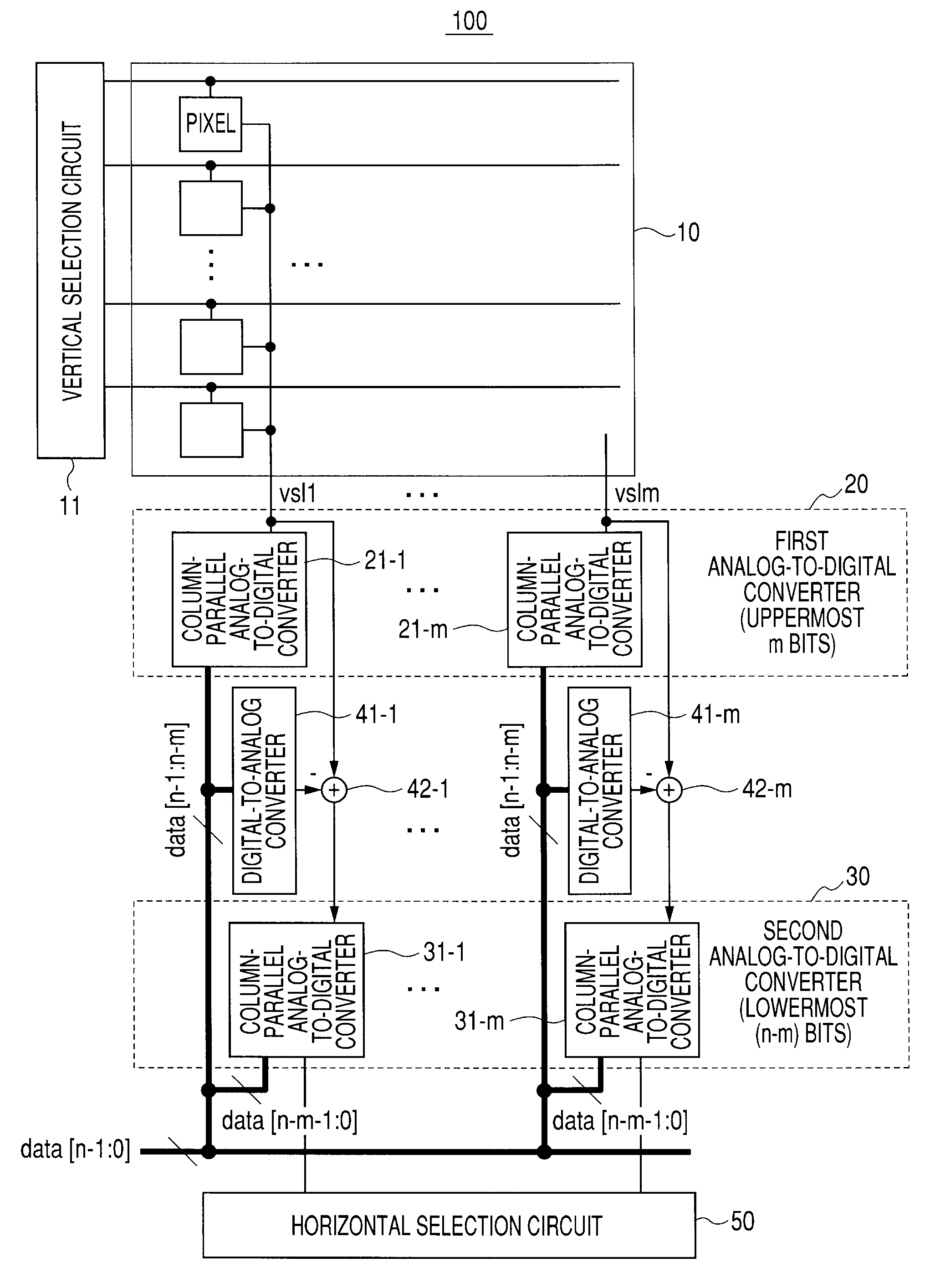
[0042]FIG. 1 is a diagram illustrating the block structure of a solid-state imaging device 100 including a column-parallel analog-to-digital converter according to an embodiment of the invention.

[0043]The solid-state imaging device 100 includes a pixel unit 10 which will be described later, a first uppermost m-bit analog-to-digital converter 20, a second lowermost (n−m)-bit analog-to-digital converter 30 (where, m and n are arbitrary positive integers and n is larger than m), a timing signal generator (not shown), a vertical selection circuit 11, and a horizontal selection circuit 50.

[0044]The timing signal generator (not shown) receives a vertical synchronization signal, a horizontal synchronization signal, a sensor driving clock, and a sensor reset signal from the external of a sensor of the solid-state imaging device 100. The timing signal generator generates a timing signal so as to drive the vertical selection circuit 11, the horizontal selection circuit 50, the column-parallel...


PUM


Abstract

A solid-state imaging device includes: a plurality of pixels which are arranged in a matrix; a sequential scanning device that selects each row of pixels; and an analog-to-digital conversion unit having a first analog-to-digital converter that is connected to a vertical signal line to which a pixel signal is supplied from the pixel and performs a first bit-length analog-to-digital conversion on an output signal from the vertical signal line or a pixel output signal obtained by sampling the output signal, and a second analog-to-digital converter that, when the first analog-to-digital converter completes the conversion operation, subtracts an analog signal corresponding to the first bit-length from the pixel output signal and then performs a second bit-length analog-to-digital conversion.

Description

CROSS REFERENCES TO RELATED APPLICATIONS[0001]The present invention contains subject matter related to Japanese Patent Application JP 2006-059857 filed in the Japanese Patent Office on Mar. 6, 2006, the entire contents of which being incorporated herein by reference.BACKGROUND OF THE INVENTION[0002]1. Field of the Invention[0003]The invention relates to a solid-state imaging device including column-parallel analog-to-digital converters provided to outputs of a plurality of vertical signal lines and capable of moderating device accuracy and reducing a conversion time, to a method of driving the solid-state imaging device, and to a camera.[0004]2. Description of the Related Art[0005]As shown in FIG. 8, a known solid-state imaging device 400 including a column-parallel analog-to-digital converter generally uses a counter-ramp-type analog-to-digital converter using a single slope.[0006]The operation of the analog-to-digital converter shown in FIG. 8 will be described with reference to a...

Claims


Application Information

Patent Timeline
Patent Type & Authority Patents(United States)
IPC IPC(8): H04N5/335H03M1/12H03M1/66H01L27/146H03M1/14H03M1/56H04N5/369H04N5/374H04N5/378
CPCH04N5/335H04N5/378H03M1/145H04N25/00H04N25/75H04N25/77
Inventor SATO, HIROKI
Owner SONY SEMICON SOLUTIONS CORP
Why Eureka
Try Eureka