Transistor and process of producing the same, light-emitting device, and display

a technology of light-emitting devices and transistors, applied in the direction of discharge tubes/lamp details, nanoinformatics, discharge tubes/lamp details, etc., can solve the problems of not always providing the above transistor action of metal/semiconductor layered structures, difficult to reduce the channel length to below several micrometers, etc., to achieve simple structure, increase the on/off ratio, and increase the current modulation

Inactive Publication Date: 2012-02-21
OSAKA UNIV +3
View PDF9 Cites 7 Cited by
  • Summary
  • Abstract
  • Description
  • Claims
  • Application Information

AI Technical Summary

Benefits of technology

[0012]According to this invention, the semiconductor layer is situated between the emitter electrode and the collector electrode, and the sheet base electrode is situated within the semiconductor layer, so that when a collector voltage is applied to between the emitter electrode and the collector electrode and a base voltage is applied to between the emitter electrode and the base electrode, charges (electrons or holes) injected from the emitter electrode are significantly accelerated and pass through the base electrode due to the base voltage applied and arrive at the collector electrode. Namely, by applying a base voltage, it is possible to amplify the current flowing between the emitter electrode and the collector electrode. Furthermore, according to this invention, the sheet base electrode is formed on the entire surface of the semiconductor layer to such a thickness that the base electrode accelerates, due to the base voltage, the charges supplied from the emitter electrode to make them into ballistic electrons or holes, and that the ballistic electrons or holes can easily pass through the base electrode and enter into the semiconductor layer situated on the collector electrode side, so that the charges are significantly accelerated on the entire surface of the sheet base electrode and that the accelerated charges can easily pass through the base electrode. On the other hand, we found the following in the course of our studies. When the base electrode is not in sheet form (i.e., when the base electrode has discontinuities such as holes or cracks), the charges injected from the emitter electrode are not so accelerated at the discontinuities, and the charges not so accelerated cannot easily pass through the base electrode. Consequently, the current flowing between the emitter electrode and the collector electrode cannot be amplified so much, as a whole, and, moreover, the increase of the current varies depending on position. Therefore, according to the transistor of the present invention, there can be stably obtained current amplification effects comparative to those of bipolar transistors.
[0063]According to the light-emitting device of the present invention, the first or the second transistor in the light-emitting device comprises an organic EL layer between the base electrode and the collector electrode, and the organic EL layer comprises at least one luminescent layer, so that the light-emitting device can achieve surface light emission with a large current. In the production of the light-emitting device, a micro-patterning process is not necessary to make the base electrode unlike in the production of conventional SIT structures. Moreover, the light-emitting device can attain large current modulation at low voltages and has an increased ON / OFF ratio. The light-emitting device of the invention is thus simple in structure and is practical.

Problems solved by technology

This is because it is not easy for the present organic FETs to allow currents large enough to switch organic EL devices, current-driven devices, to flow.
However, with patterning techniques useful for the mass production of displays, it is difficult to decrease the channel length to below several micrometers.
However, the semiconductor / metal / semiconductor layered structure has not always provided the above transistor action.Non-Patent Document 1: S. Fujimoto, K. Nakayama and M. Yokoyama, Appl. Phys. Lett., 87, 133503 (2005).

Method used


Image

  • Transistor and process of producing the same, light-emitting device, and display
  • Transistor and process of producing the same, light-emitting device, and display
  • Transistor and process of producing the same, light-emitting device, and display

Examples


Embodiment Construction

[0085]A transistor, a process of producing it, a light-emitting device and a display according to the present invention will be described hereinafter in the order of a first transistor, a second transistor, a process of producing the second transistor, a light-emitting device, and a display. The present invention is not limited to the following embodiments and is susceptible to modification without departing from the spirit of this disclosure and the scope of the appended claims.

[0086](First Transistor)

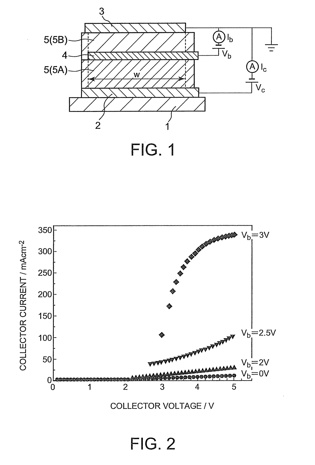
[0087]FIG. 1 is a schematic cross-sectional view of a first transistor of the present invention. A first transistor 10 of the invention comprises an emitter electrode 3, a collector electrode 2, and a semiconductor layer 5 (5A, 5B) and a sheet base electrode 4 between the emitter electrode 3 and the collector electrode 2, as shown in FIG. 1. Specifically, the semiconductor layer 5 is composed of a first semiconductor layer 5A situated between the collector electrode 2 and the base ele...


PUM

PropertyMeasurementUnit
thicknessaaaaaaaaaa
lengthaaaaaaaaaa
thicknessaaaaaaaaaa

Abstract

A transistor capable of modulating, at low voltages, a large current flowing between an emitter electrode and a collector electrode. A process of producing the transistor, a light-emitting device comprising the transistor, and a display comprising the transistor. The transistor comprises an emitter electrode and a collector electrode. Between the emitter electrode and the collector electrode are situated a semiconductor layer and a sheet base electrode. It is preferred that the semiconductor layer be situated between the emitter electrode and the base electrode and also between the collector electrode and the base electrode to constitute a second semiconductor layer and a first semiconductor layer, respectively. It is also preferred that the thickness of the base electrode be 80 nm or less. Furthermore, a dark current suppressor layer is situated at least between the emitter electrode and the base electrode, or between the collector electrode and the base electrode.

Description

BACKGROUND OF THE INVENTION[0001]1. Field of the Invention[0002]The present invention relates to a transistor, a process of producing it, to a light-emitting device, and to a display. More particularly, the present invention relates to a transistor capable of modulating, at low voltages, a large current flowing between the emitter and the collector, to a process of producing the transistor, to a light-emitting device comprising the transistor, and to a display comprising the transistor.[0003]2. Background Art[0004]Although some displays using organic transistors, produced on an experimental basis, have been reported in recent years, many of them are combinations of organic field-effect transistors (organic FETs) and liquid crystals or electrophoretic cells, and there have been reported few displays using organic EL devices. This is because it is not easy for the present organic FETs to allow currents large enough to switch organic EL devices, current-driven devices, to flow. There i...

Claims


Application Information

Patent Timeline
Patent Type & Authority Patents(United States)
IPC IPC(8): H01L51/52
CPCB82Y10/00H01L27/3262H01L51/5296H01L51/0504H01L51/5203C08G2261/92H01L51/0037H01L51/0046H01L51/0053H01L51/0078H01L51/0081H01L51/5096H01L51/006H10K59/1213H10K85/211H10K85/1135H10K85/621H10K85/633H10K85/311H10K85/324H10K10/00H10K50/18H10K50/805H10K50/30H10K2102/351
Inventor YOKOYAMA, MASAAKINAKAYAMA, KENICHI
Owner OSAKA UNIV
Why Eureka
Try Eureka