

Switching power supply with switching circuits
a technology of switching circuit and power supply, which is applied in the direction of power conversion systems, dc-dc conversion, instruments, etc., can solve the problems of insufficient manufacturing cost and size of switching power supply
- Summary
- Abstract
- Description
- Claims
- Application Information
AI Technical Summary
Benefits of technology
Problems solved by technology
Method used
Image

Examples
first embodiment
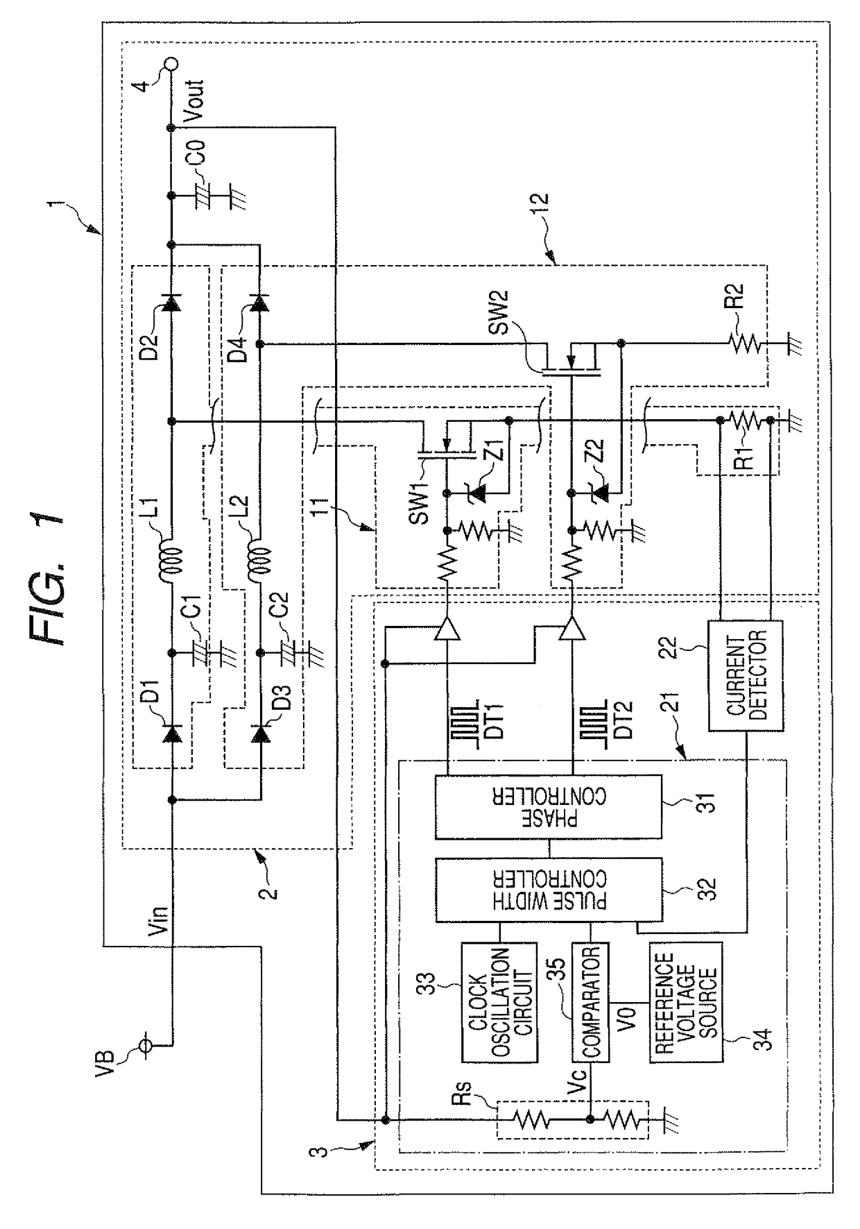
[0021]FIG. 1 is a circuit view of a switching power supply according to the first to fourth embodiments.
[0022]As shown in FIG. 1, a switching power supply 1 disposed in an electronic control unit (ECU) of a vehicle has a voltage boosting unit 2 and a control unit 3. The boosting unit 2 receives an input voltage Vin of a direct current from a battery VB such as an external electric power source, boosts this voltage Vin to an output voltage Vout and outputs the voltage Vout. The input voltage Vin is changeable in response to cranking or cranking return. The control unit 3 controls the boosting unit 2 to outputs the voltage Vout adjusted at a target value (e.g., 8V) even when the input voltage Vin is dropped or returned to a normal value.
[0023]The boosting unit 2 has two switching circuits 11 and 12 connected parallel to each other, a capacitor C0 having both a first terminal connected with a common point of the circuits 11 and 12 and a second terminal earthed, and an output terminal 4...
second embodiment
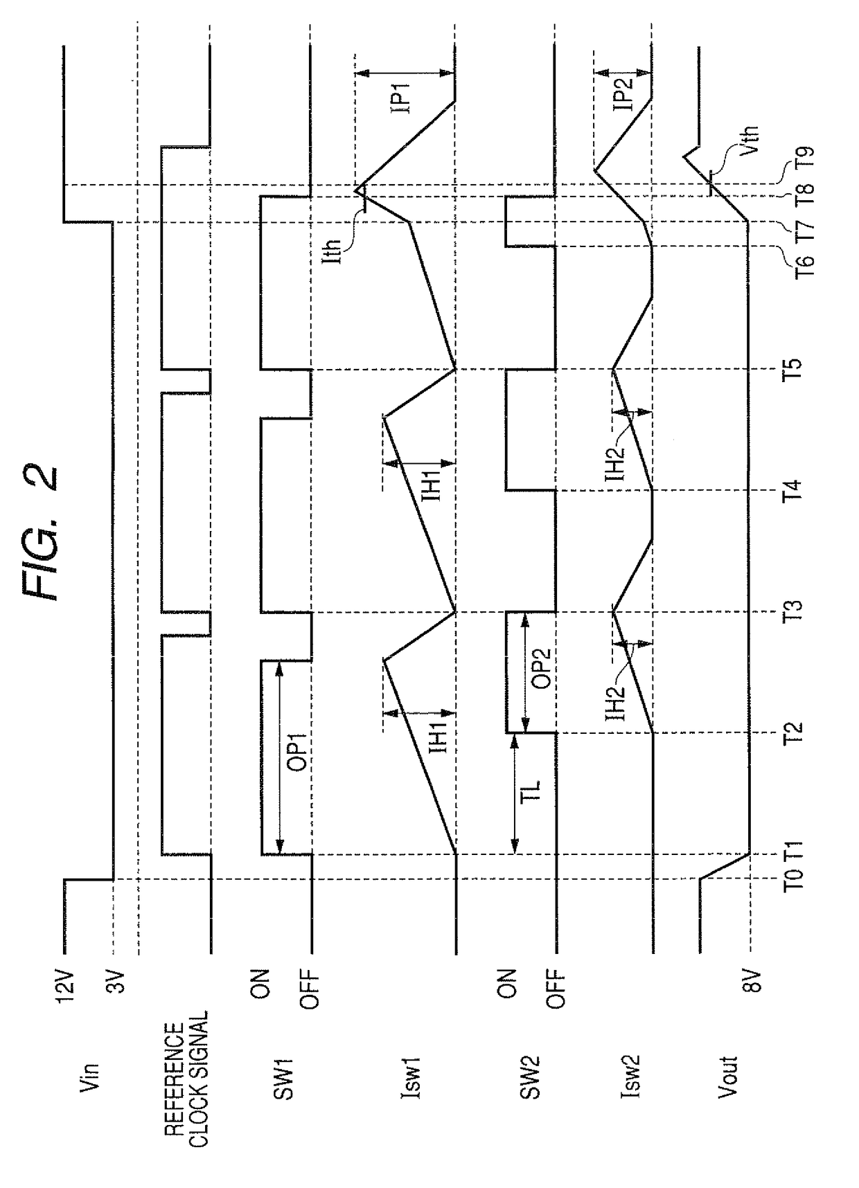
[0060]There is a case where the input voltage Vin lowered to the lower voltage value (e.g., 3V) is gradually heightened to the normal voltage value (e.g., 12V). In this case, the current Isw1 of the switching element SW1 is gradually increased to a current limiting value and reaches the upper current limit Ith higher than the current limiting value. In this case, when the current Isw1 reaches the current limiting value lower than the limit Ith, it is preferable that the on-state period in each of the elements SW1 and SW2 be shortened for a short time, before being set at zero value, to slightly reduce the currents Isw1 and Isw2.
[0061]In this embodiment, only this current limiting process differs from that according to the first embodiment.
[0062]FIG. 4 is a flow chart showing the current limiting process according to the second embodiment.
[0063]As shown in FIG. 4, at step S110, the controller 32 judges whether or not the switching current Isw1 detected in the detector 22 is equal to ...
third embodiment
[0071]In the first embodiment, the resistance value of the resistor R2 is set to be higher than the resistance is value of the resistor R1, so that the current Isw2 of the element SW2 reliably becomes lower than the current Isw1 of the element SW1.
[0072]In contrast, in the third embodiment, to reliably obtain the current Isw2 of the element SW2 lower than the current Isw1 of the element SW1, the controller 32 sets a first on-pulse width OP11 of the duty signal DT1 and a second on-pulse width OP12 of the duty signal DT2 such that the width OP12 is shorter than the width OP11. For example, the width OP12 is set to be half of the width OP11. Further, the resistance value of the resistor R2 is, for example, set to be substantially equal to the resistance value of the resistor R1. Moreover, for example, the controller 32 sets the duty signals DT1 and DT2 such that each pulse of the signal DT2 has the leading edge at the same timing as the leading edge of one pulse of the signal DT1.
[0073...
PUM
 Abstract
Description
Claims
Application Information