ID label, ID card, and ID tag

a technology of id labels and tags, applied in the field of id labels, id cards, id tags, etc., can solve the problems of limit design and inevitable increase in manufacturing costs, and achieve the effects of low cost, superior functionality, and thin shap

Active Publication Date: 2012-03-20
SEMICON ENERGY LAB CO LTD
View PDF70 Cites 189 Cited by
  • Summary
  • Abstract
  • Description
  • Claims
  • Application Information

AI Technical Summary

Benefits of technology

[0008]However, as a contact and a non-contact IC chips are widespread, it is required to manufacture a large quantity of IC chips which can be used for people, plants and animals, products, paper money at quite a low cost. An IC chip attached to products, paper money and the like is, for example, required to be manufactured at a cost of one to several yens each, or preferably less than one yen. Thus, such a structure and a process of an integrated circuit device such as an IC chip are demanded so that it can be manufactured in a large quantity at a low cost.
[0017]A thin film integrated circuit device of each of the aforementioned ID label, the ID card, and the ID tag according to the invention comprises a thin film active element such as a thin film transistor (TFT). In the case of manufacturing a thin film integrated circuit device using a TFT, for example, after forming a TFT on a substrate which is to be peeled off, the substrate is peeled off to separate the elements, thereby a thin film integrated circuit device formed of a TFT can be manufactured in a large quantity at a low cost. The major peeling methods here are a chemical peeling that a peeling layer is removed by etching and the like, and a physical peeling that a peeling layer is separated by applying a pressure externally, however, the invention is not limited to these.
[0024]The ID tag functions to identify a product that circulates in the market and to store the data on them similarly to the ID label. By providing the ID label or the ID tag to the product, products can be easily managed. In the case where a product is stolen, for example, a criminal can be rapidly grasped by tracking the route of the product. In this manner, by providing the ID tag, products which is superior in so-called traceability (when a problem occurs in each stage of complicated manufacture and circulation, the cause can be rapidly figured out by tracking the route) can be circulated. Moreover, as recently accidents such as violent crime and disappearance increase, the ID tag can be used for identifying a person in order to constantly figure out a location of each person such as an infant, a child, an aged, a traveler so that they will not be involved in the accidents.
[0030]The thin film integrated circuit device included in the ID label, the ID card, or the ID tag according to the invention includes a thin film active element such as a TFT. After forming a TFT on a substrate that is to be peeled off, the substrate is peeled off to separate the element, thereby the thin film integrated circuit device can be manufactured in a large quantity at a low cost. As the thin film integrated circuit device comprises a thin film active element, the ID label, the ID card, and the ID tag in thinner design than a conventional technique can be obtained.
[0031]Further, as a back surface of a chip is not required to be polished unlike a conventional IC chip formed on a silicon substrate, a process can considerably be simplified and the manufacturing cost can be reduced to a large extent. Moreover, a glass substrate, a quartz substrate, a solar battery grade silicon substrate and the like which are cheaper than the silicon substrate can be used and the peeled substrate can be reutilized. Therefore, a large cost reduction can be realized.
[0033]Accordingly, various objects such as the ID label, the ID card, the ID tag and the like which can be manufactured in a large quantity at a low cost, has a thin shape, and is superior in functionality can be provided according to the invention.

Problems solved by technology

However, as a silicon wafer that is expensive is all grinded and removed, increase in manufacturing cost is inevitable.
Further, an integrated circuit formed on a silicon wafer is thick, therefore, there is a limit in design due to projections and depressions when mounting it to a package of product.

Method used


Image

  • ID label, ID card, and ID tag
  • ID label, ID card, and ID tag
  • ID label, ID card, and ID tag

Examples


embodiment mode 1

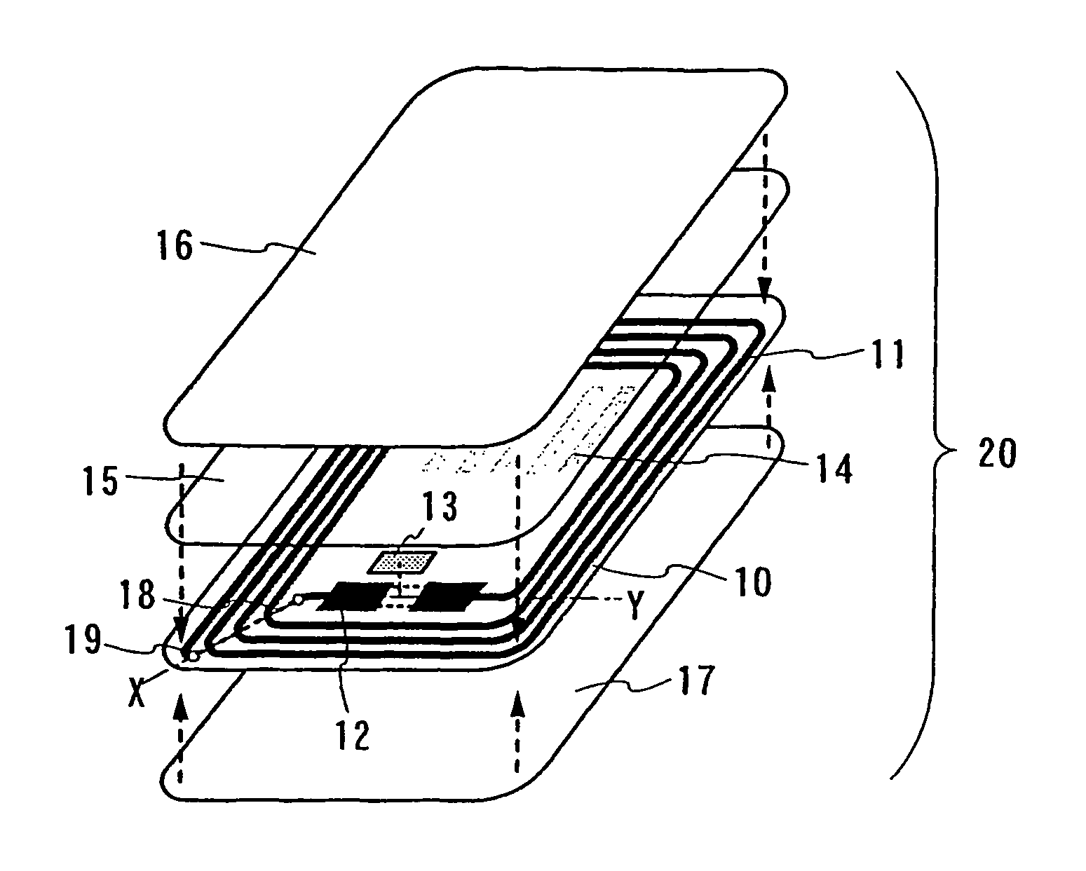
[0071]A structure and a manufacturing method of the ID label 20 of the invention are described mainly with reference to FIGS. 1A, 2, and 3A and 3B. FIG. 1A is a perspective view showing a stacked-layer structure of the ID label according to the invention. Here, a separating sheet as a mounting of the label is shown over a label substratum (generally referred to as “tack paper” and the like, though not limited to a paper material) adhered to a product and the like.

[0072]In FIG. 1A, an antenna 11 and a connecting pad 12 which is a connecting portion between the antenna and the thin film integrated circuit device are formed on a label substratum 10 and a thin film integrated circuit device 13 formed separately is adhered to the label substratum. A print 14 such as text, a sign, and an image is applied on a surface (a back surface in FIG. 1A) of the label substratum. Moreover, in the case of forming so-called a hybrid type ID label which has both non-contact and contact functions, a wir...

embodiment mode 2

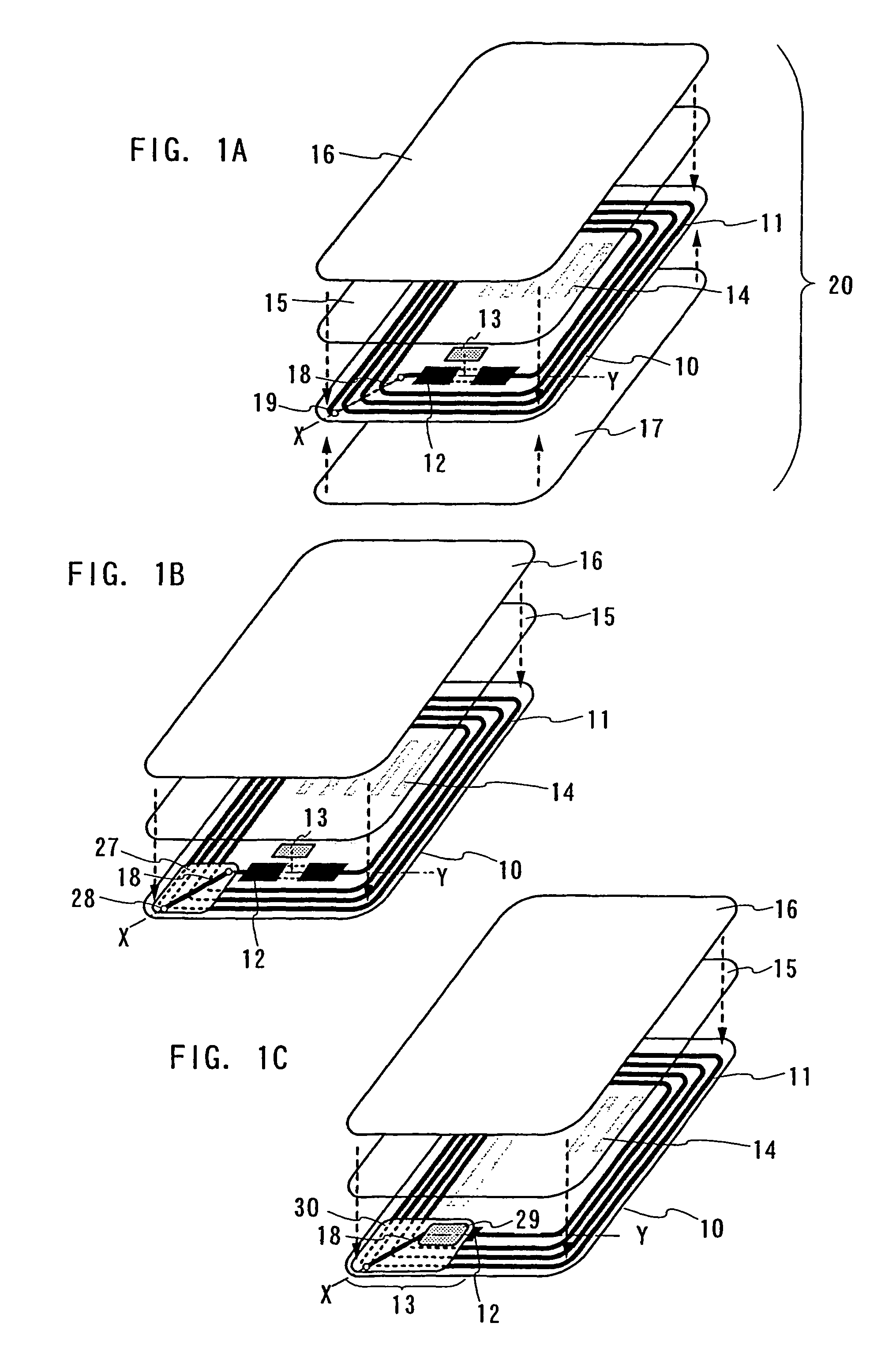
[0090]A structure and a manufacturing method of the ID label according to the invention are described mainly with reference to FIGS. 1B, 4A and 4B. FIG. 1B is a perspective view showing a stacked-layer structure of the ID label of the invention. Here for simplicity, a separating sheet as a mounting of the label is shown over a label substratum which is adhered on a product and the like.

[0091]FIG. 1B is similar to FIG. 1A in the respect that the antenna 11 and the connecting pad 12 which is a connecting portion between the antenna and a thin film integrated circuit are formed in advance on the label substratum 10 and a thin film integrated circuit 13 which is separately formed is adhered on the label substratum 10. However, in FIG. 1B, the cross wiring 18 which connects the thin film integrated circuit device and the antenna is formed on an insulating layer over the label substratum.

[0092]In this case, an insulating layer 27 is provided so that the antenna 11 and the cross wiring 18 ...

embodiment mode 3

[0098]A structure and a manufacturing method of the ID label according to the invention is described mainly with reference to FIGS. 1C and 4B. FIG. 1C is a perspective view showing a stacked-layer structure of the ID label of the invention. Here for simplicity, a separating sheet as mounting of the ID label is shown over a label substratum which is adhered on a product and the like.

[0099]FIG. 1C is similar to FIG. 1A in the respect that the antenna 11 and the connecting pad 12 which is a connecting portion between the antenna and a thin film integrated circuit are formed in advance on the label substratum 10 and the thin film integrated circuit 13 which is separately formed is adhered on the label substratum 10. However, in FIG. 1C, the cross wiring 18 which connects the thin film integrated circuit device and the antenna is formed inside the thin film integrated circuit device.

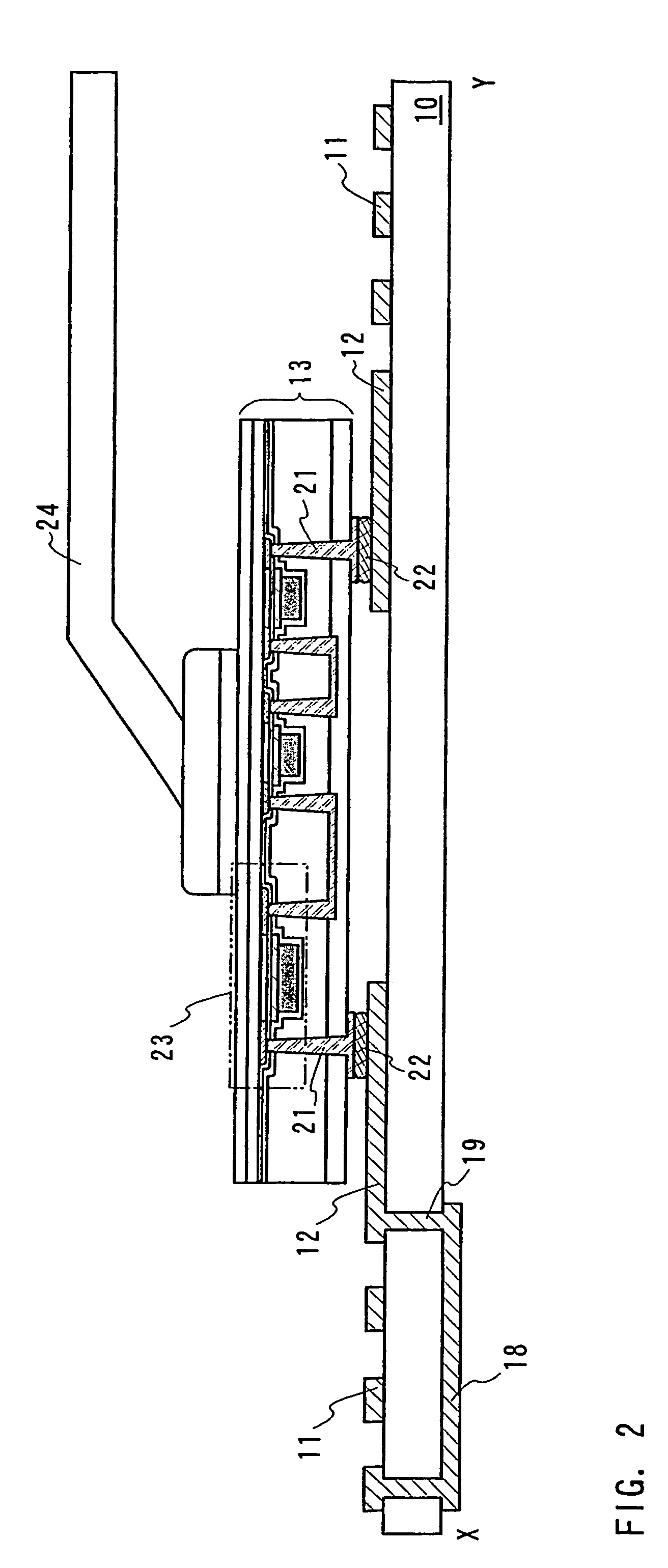
[0100]FIG. 4B is a cross sectional view along X-Y in FIG. 1C. Connecting wirings 21a to 21c which are conn...


PUM


Abstract

As a non-contact ID label, ID tag and the like being widespread, it is required to manufacture a considerable quantity of ID labels at quite a low cost. An ID label attached to a product is, for example, required to be manufactured at 1 to several yens each, or preferably less than one yen. Thus, such a structure and a process are demanded that an ID label can be manufactured in a large quantity at a low cost. A thin film integrated circuit device included in the ID label, the ID card, and the ID tag of the invention each includes a thin film active element such as a thin film transistor (TFT). Therefore, by peeling a substrate on which TFTs are formed for separating elements, the ID label and the like can be manufactured in a large quantity at a low cost.

Description

TECHNICAL FIELD[0001]The invention relates to an ID label, an ID card, and an ID tag each of which comprises a memory, a micro processor (a central processing unit and MPU) and the like, a quite thin film integrated circuit, and is used for identifying mainly a person, plants and animals, products and the like.BACKGROUND ART[0002]In recent years, safety of the products and reinforcement of management control are increasingly demanded in all industrial fields such as food industry and manufacturing industry, and data on products are increasing accordingly. The data on products for the present are very little mainly such as a country of manufacture, a manufacturer, product number and the like provided by a ten-digit number of a bar code. Further, a bar code has to be read one by one manually, which requires time. Now, an automatic identification technique using a non-contact IC tag utilizing radio wave, which is called an RFID (Radio Frequency Identification) is attracting attentions....

Claims


Application Information

Patent Timeline
Patent Type & Authority Patents(United States)
IPC IPC(8): G06K19/06G06K19/00G06K19/02B42D15/10G06K19/07G06K19/077G09F3/00H01L21/77H01L21/84H01L27/12H01L27/13H01L29/786
CPCG06K19/07718G06K19/0775G06K19/07779G06K19/07783H01L27/1203H01L27/1214H01L27/1266H01L27/13G06K19/07749H01L2924/01021H01L29/78603H01L2224/83192H01L2924/01004H01L2924/0102H01L2924/01025H01L2924/01046H01L2924/01077H01L2924/01078H01L2924/01079H01L2924/01019
Inventor ARAI, YASUYUKIAKIBA, MAITACHIMURA, YUKOKANNO, YOHEI
Owner SEMICON ENERGY LAB CO LTD
Why Eureka
Try Eureka