Programmable delay introducing circuit in self timed memory

a delay and self-timed technology, applied in the field of self-timed memories, can solve problems such as delay introduced in the triggering of sense amplifiers, and achieve the effect of extending the delay

Active Publication Date: 2012-03-20
STMICROELECTRONICS INT NV
View PDF6 Cites 0 Cited by
  • Summary
  • Abstract
  • Description
  • Claims
  • Application Information

AI Technical Summary

Benefits of technology

[0015]Another object of the present invention is to provide delay introducing circuitry that introduces a delay in a sense amplifier enable signal that is a function of memory cell spice characteristics and the core parasitic capacitances.
[0018]Since idle-lying metal capacitances are utilized, extra hardware is not required. Thus, in the configuration as disclosed by the present invention, there is minimal area overhead in an area required only for the switches used and the switch control signals generation in the circuitry.
[0020]Another feature of the proposed circuitry is that it provides a delay that increases with the number of rows of a cut. A cut with larger number of rows needs a larger delay than that with a smaller number of rows to generate the same voltage differential, which is sufficient for a correct evaluation by the sense amplifier. Hence, the circuit provided by the present invention performs intelligent adaptation of delays with the number of rows in the cut.

Problems solved by technology

Therefore, delay introduced in triggering of the sense amplifiers may depend on the delay introduced in the RESET signal.

Method used


Image

  • Programmable delay introducing circuit in self timed memory
  • Programmable delay introducing circuit in self timed memory
  • Programmable delay introducing circuit in self timed memory

Examples


Embodiment Construction

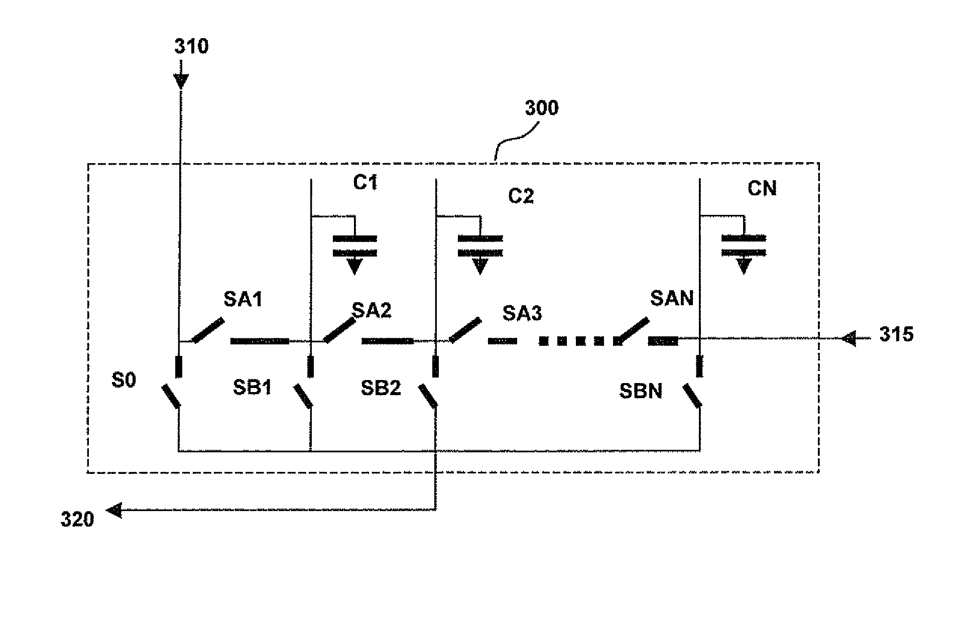
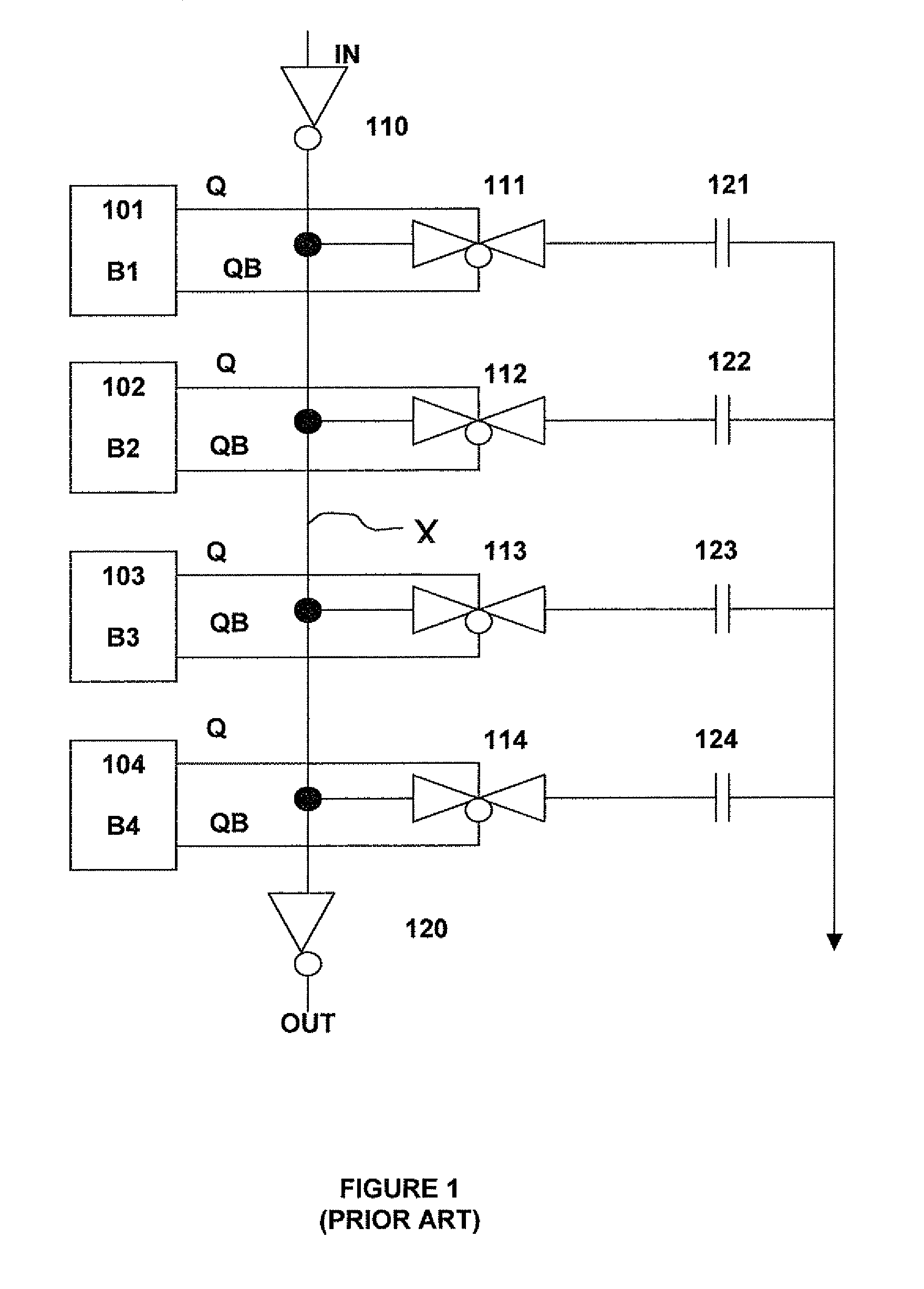
[0025]FIG. 1 shows a block diagram of a programmable delay element as used in the field. The circuit comprises memory cells (101), (102), (103) and (104) which are loaded with bits B1, B2, B3 and B4. An inverter (110) drives internal node X. Capacitors (121), (122), (123) and (124) are connected to node X via transmission gates (111), (112), (113) and (114). The capacitors (121), (122), (123) and (124) have capacitances C1, C2, C3 and C4. The transmission gates (111), (112), (113) and (114) are controlled by memory cells (101), (102), (103) and (104) respectively. The Q output terminals of the memory cells (101), (102), (103) and (104) are coupled to the gates of the NMOS transistors of the transmission gates (111), (112), (113) and (114) respectively. The QB output terminals of the memory cells (101), (102), (103) and (104) are coupled to the gates of the PMOS transistors of transmission gates (111), (112), (113) and (114) respectively.

[0026]A transmission gate is on if there is lo...


PUM


Abstract

A novel method for introducing delays in self timed memories is disclosed. In the proposed method, delays are introduced by introducing a capacitance on the path of signal to be delayed. The capacitances are realized by using idle lying metal layers in the circuit. The signal to be delayed is connected to these idle lying capacitances via programmable switches. The amount of delay introduced depends on the capacitance introduced in the path of signal which in turn depends on state of the switches. The state of the switches is controlled by delay codes provided externally to the delay introducing circuitry. Since, in the proposed method, idle-lying metal capacitances are utilized, the circuit can be implemented using minimum amount of additional hardware. Also delay provided by the proposed circuitry is a function of memory cell spice characteristics and core parasitic capacitances.

Description

FIELD OF THE INVENTION[0001]The present invention relates to the field of self-timed memories, and more particularly, to a method and circuit for providing delay codes in a self-timed memory.BACKGROUND OF THE INVENTION[0002]A semiconductor memory is composed of data storage cells arranged in rows and columns. At the time of reading from or writing into a memory, a set of external control signals and clocks are activated. The memory cells from which the data is to be read / written are accessed and then the data is read (or written) by the read (or write) circuitry. The read circuitry performs the reading operation by sensing the voltage difference developed across the bit lines (or data lines).[0003]To ensure that desired data is read correctly, the read operation at the sense amplifier should be triggered only when sufficient voltage differential has been developed across the bit lines. This is done by ensuring a time delay between accessing a memory cell and triggering the amplifier...

Claims


Application Information

Patent Timeline
Patent Type & Authority Patents(United States)
IPC IPC(8): H05B1/02
CPCG11C7/06G11C7/08G11C7/22G11C7/222G11C7/227G11C29/14G11C29/50G11C29/50012G11C29/12015
Inventor KOHLI, NISHUBHARGAVA, MUDITKUMAR, SHISHIR
Owner STMICROELECTRONICS INT NV
Why Eureka
Try Eureka