Method and apparatus for on-the-fly minimum power state transition

a technology of power state transition and power state, applied in the direction of logic circuits, pulse techniques, instruments using specific components, etc., can solve the problems of secondary power consumption in energy to cool the ic, degrade ic performance and reliability, and leakage reduction, so as to reduce the overhead of implementing the novel sleep mode operation and reduce the power consumption required

Inactive Publication Date: 2011-05-24
GLOBALFOUNDRIES INC
View PDF10 Cites 5 Cited by
  • Summary
  • Abstract
  • Description
  • Claims
  • Application Information

AI Technical Summary

Benefits of technology

[0011]To that end, the present invention provides a design structure that implements novel improved input vector control (IVC), in a method referred to as “on-the-fly minimum power transition.” The novel “on-the-fly minimal power transition” method, and the design structure that enables same takes advantage of the fact that large portions of microprocessor logic is comprised of pipelines and quiescent functional units that need not be restored to their pre-sleep mode state when exiting from low power or sleep mode states. In many cases, it is sufficient to reset latches with the same logical values that the flip-flops are set to at initialization. Hence, the inventive structure and method takes advantage of existing logic circuits for initialization. This invention inserts an IVC circuit in IC scan path to apply the input vector to be set for IVC in just one cycle. The IVC circuit also allows exiting sleep mode and reinitializing the latch in one additional cycle. This reduces the power consumption required to enter and exit the sleep mode. The area overhead for implementing the novel sleep mode operation is minimal as well.
[0012]The inventive structure and associated VLSI designs shows no timing degradation in the critical paths as found in prior art attempts to minimize power loss using IVC schemes. The inventive structure may be seamlessly integrated in standard design flows. That is, the benefit of using the novel structure and method in VLSI design realizes a resulting reduction in the dynamic power consumption of the scan chains (i.e., switching power is eliminated during functional operation), and a fast transition in / out of the low leakage state. Fast transition in and out of leakage state realizes marked decrease in consumed power due to minimized latch toggling. And as known, for testability reasons, the scan paths cover almost every latch in a microprocessor design. Thus, during normal operational mode, there is minimal unnecessary toggling or switching, and less global power dissipation throughout the IC therefore.

Problems solved by technology

Power leakage reduction in VLSI processors is not just an issue for operation and performance, but in manufacturing as well.
For that matter, leakage power consumption for normal operation causes a secondary power consumption in energy to cool the IC as a consequence.
If not cooled, increased temperature conditions can degrade IC performance and reliability.
The cited references appear to agree that leakage power consumption within an IC device depends strongly on the state of the IC device input and of the internal memory elements (e.g. latches), which affects switching and leakage significantly.
The Abdollahi approach, however, has its drawbacks.
For example, the suggested approach introduces additional logic in the critical circuit or logic paths, which degrades or slows timing.
This results in a large routing overhead in the original circuit floorplan, where the fan-out tree itself consumes significant static and dynamic power each time the additional logic path sets and resets the sleep mode.
Hence, the second Abdollahi technique also imposes large area overhead, limiting the benefit for their stated purpose.
More, the second technique may impose other global sleep mode complications in the ICs or IC processors within which they would be implemented.
Such an approach includes an area overhead for at least the memory, and may counteract any improvement in stemming current leakage that could be realized.
That is, implementing such an approach in an existing IC or processor design would require modifying flip-flop design globally, and would therefore be disruptive in the design's manufacturing process.
Required redesign would be likely to negatively impact project scheduling when the modified flip-flops are incorporated into existing designs.
Moreover, the new proposed flip-flops would be inherently slower because of the third latch, so that overall timing during normal operational mode would be adversely affected, further complicating redesign efforts.

Method used


Image

  • Method and apparatus for on-the-fly minimum power state transition
  • Method and apparatus for on-the-fly minimum power state transition
  • Method and apparatus for on-the-fly minimum power state transition

Examples


Embodiment Construction

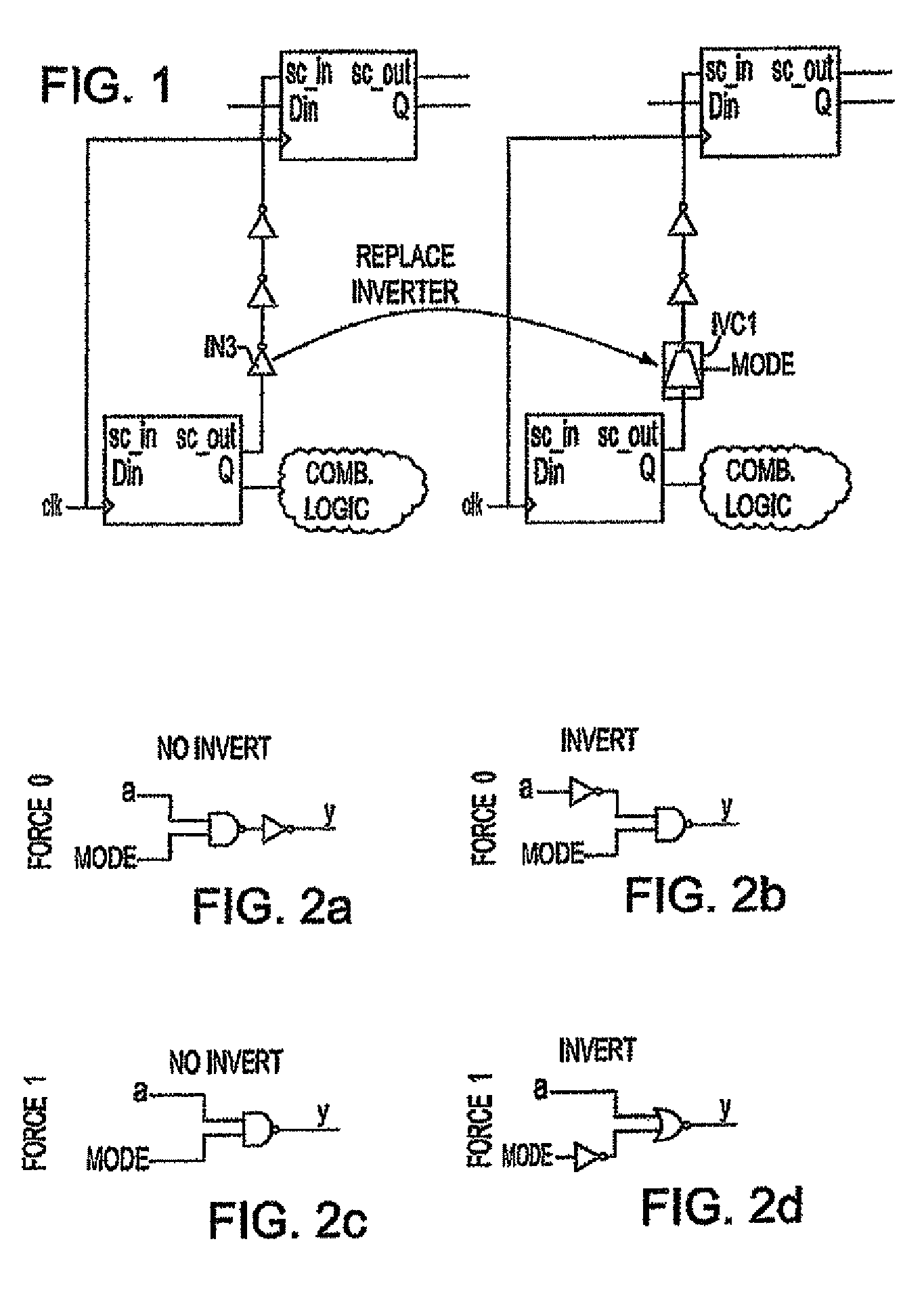
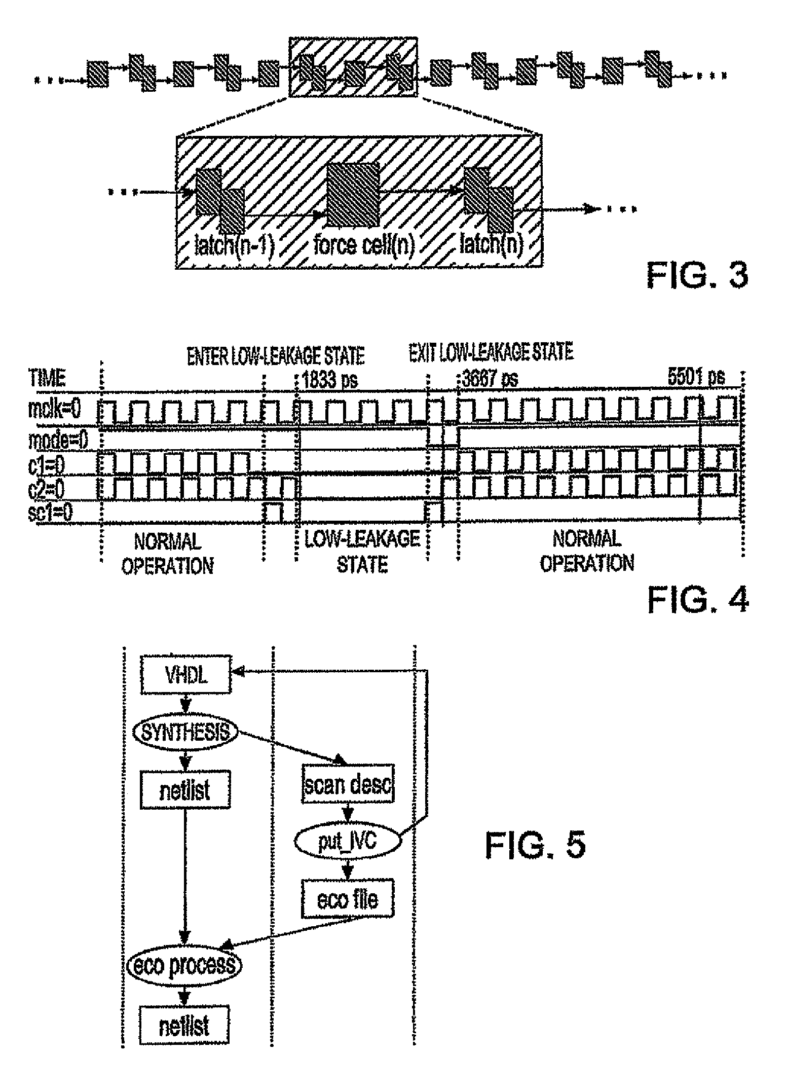
[0021]At initialization, many conventional VLSI designs, i.e., microprocessors, do not initialize their flip-flops with a global reset, which would require routing a global signal and consequential degrading of the flip-flop timing. Such conventional designs instead use the scan-path to force an initial value at flip-flops, such as that design disclosed in commonly owned U.S. Pat. No. 7,100,144. Hence, in order to reset N latches, the conventional scan-path approaches require circa N clock cycles. The drawback is that where N is very large (which it is in many typical VLSI microprocessor designs), initialization time becomes critical, particularly in certain applications (e.g., Telco market, real time applications, etc).

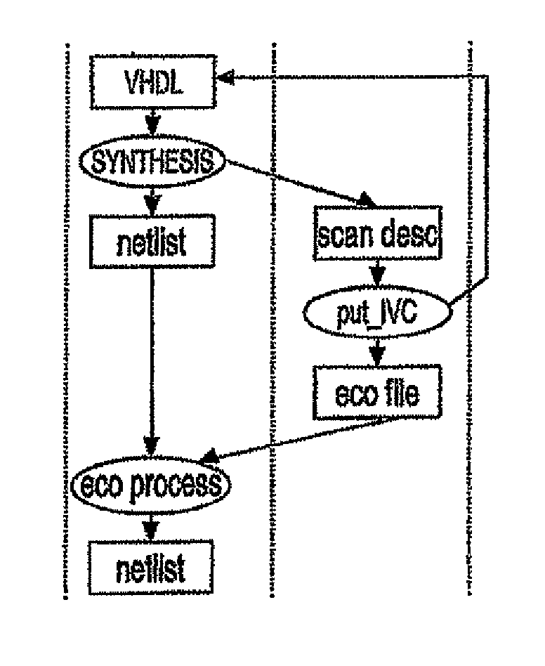
[0022]The inventive method and VLSI scan chain structure disclosed herein provide for an improved level sensitive scan design (LSSD) or scan-path approach. The novel approach may be described broadly as “on-the-fly minimum power transition”. The “on-the-fly minimum p...


PUM


Abstract

The invention includes a design structure embodied in a computer readable medium for performing a method for inserting a scan chain into a VLSI circuit design. The scan chain structure, or structures, are included in the design structure for the VLSI circuit design. The scan chain structure includes a first flip-flop (L1) and a second flip-flop (L2) configured to operate the first flip-flop (L1) in normal mode operation, in scan mode operation, in initialization mode and in low leakage power mode operation. A buffer circuit is electrically connected between the scan-out output of the second flip-flop (L2) and the scan-in input of the first flip-flop (L1) for the next latch in the scan chain. Buffer circuit control elements control the first flip-flop (L1) to switch between scan mode or low power leakage mode. The switching occurs in only one clock cycle. The design structure can include a netlist, which describes the VLSI circuit, reside on storage medium as a data format used for the exchange of layout data of integrated circuits, and preferably includes at least one of test data files, characterization data, verification data, or design specifications.

Description

CROSS-REFERENCE TO RELATED APPLICATIONS[0001]The present application is a continuation in part application of U.S. patent application Ser. No. 11 / 691,856, filed Mar. 27, 2007, now U.S. Pat. No. 7,757,137 B2.BACKGROUND OF THE INVENTION[0002]The present invention relates to improved power leakage control in very large scale integrated (VLSI) circuits, and more particularly relates to a design structure for fabricating a scan-based VLSI circuit with improved input vector control (IVC), by use of scan-chain logic to set sleep mode and reset flip flops comprising the scan-chain logic from a low-power state with the same logical values that the flip-flops were set to at initialization.[0003]This and related power leakage problems in VLSI processors are discussed in detail in a paper by Rohrer, et al., POWERPC 970 IN 130 NM AND 90 NM TECHNOLOGY, Pages 68-69, ISSCS 2004. Power leakage reduction in VLSI processors is not just an issue for operation and performance, but in manufacturing as we...

Claims


Application Information

Patent Timeline
Patent Type & Authority Patents(United States)
IPC IPC(8): G06F17/50H01L25/00H03K19/00
CPCG01R31/318536G01R31/318575G06F17/5045G06F2217/78G06F2217/14G06F30/30G06F30/333G06F2119/06
Inventor ORTIZ, ALBERTO GARCIALICHTENAU, CEDRICROHRER, NORMAN J.
Owner GLOBALFOUNDRIES INC
Why Eureka
Try Eureka