Surface mount package with ceramic sidewalls

a technology of sidewalls and surface mounts, applied in the direction of semiconductor devices, semiconductor/solid-state device details, electrical apparatus, etc., can solve the problems of increasing the desirability of a surface mount package, reducing the available space, and increasing the complexity of electronic devices

Inactive Publication Date: 2012-03-27
HCC AEGIS
View PDF9 Cites 13 Cited by
  • Summary
  • Abstract
  • Description
  • Claims
  • Application Information

AI Technical Summary

Problems solved by technology

As electronic devices become more complex and available space is reduced, the desirability of a surface mount package increases.
Concurrently, as the device complexity increases, the heat generated by operation increases.
If the heat is not removed, the temperature of the device rises shortening the operational life.
Aluminum nitride and silicon carbide are more expensive than alumina and more difficult to shape.
A disadvantage with this approach is that an insulative alumina layer is disposed between the integrated circuit device and the heat sink.
The removal of heat from the chip is limited by the conduction of heat through the alumina layer.
An infiltrated base has limitations.
Any air gaps will reduce thermal conductivity.
When the concentration of the tungsten is high, above about 65% by volume (80% by weight), the infiltrated composite becomes difficult to shape by forging or other deformation processes.
Machining is required, necessitating piece-by-piece manufacture and the generation of scrap increasing the cost of the composite.

Method used


Image

  • Surface mount package with ceramic sidewalls
  • Surface mount package with ceramic sidewalls
  • Surface mount package with ceramic sidewalls

Examples


Embodiment Construction

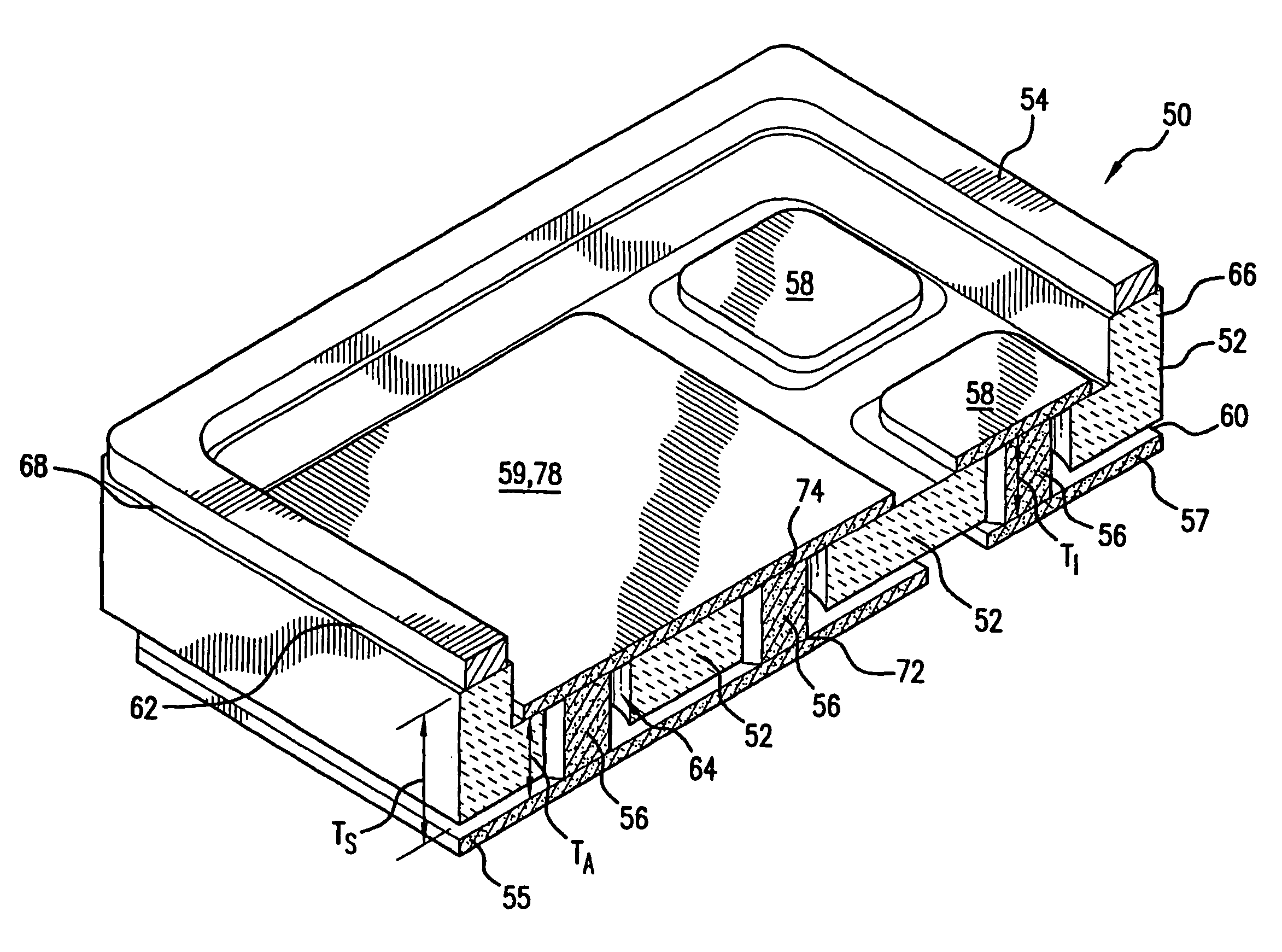
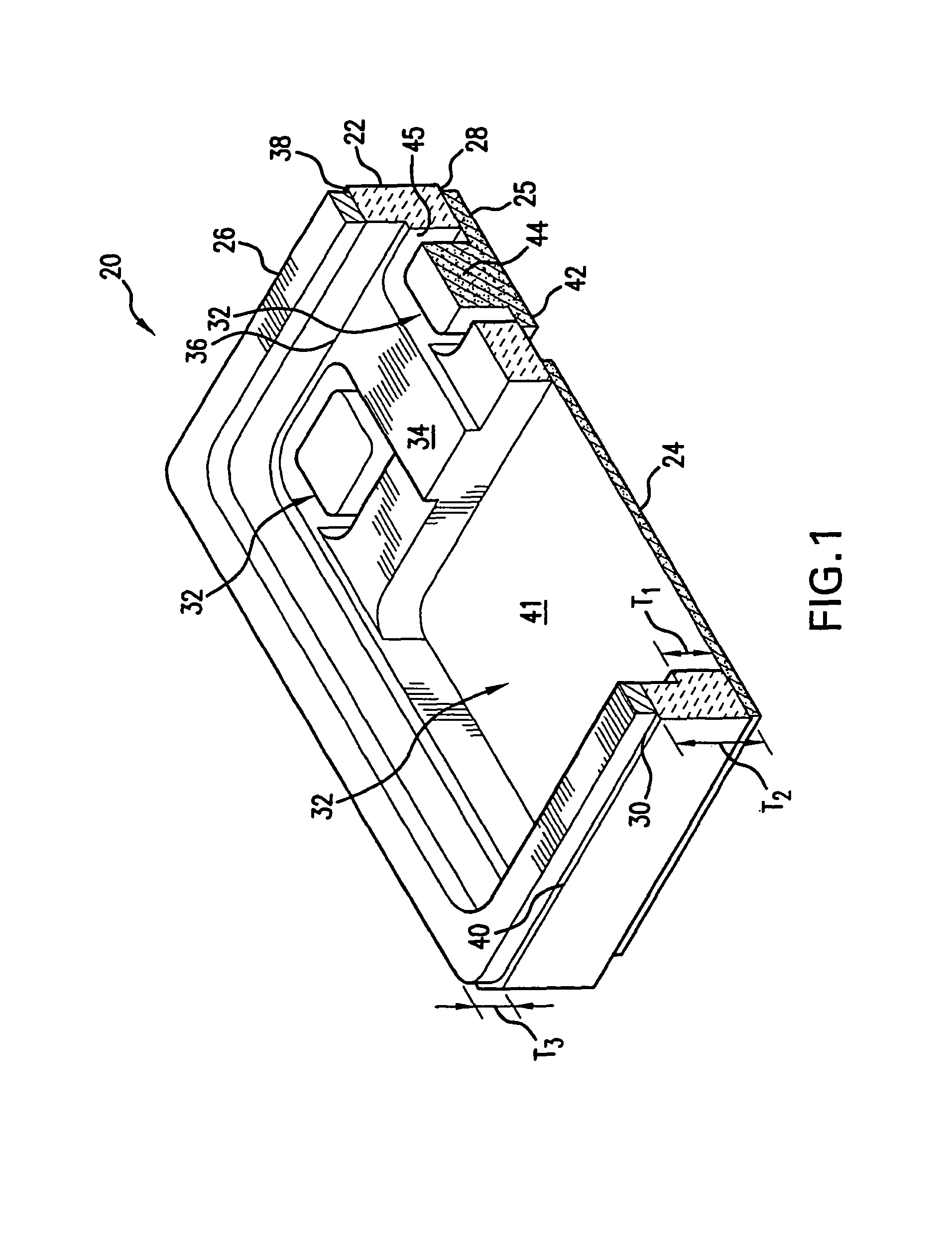
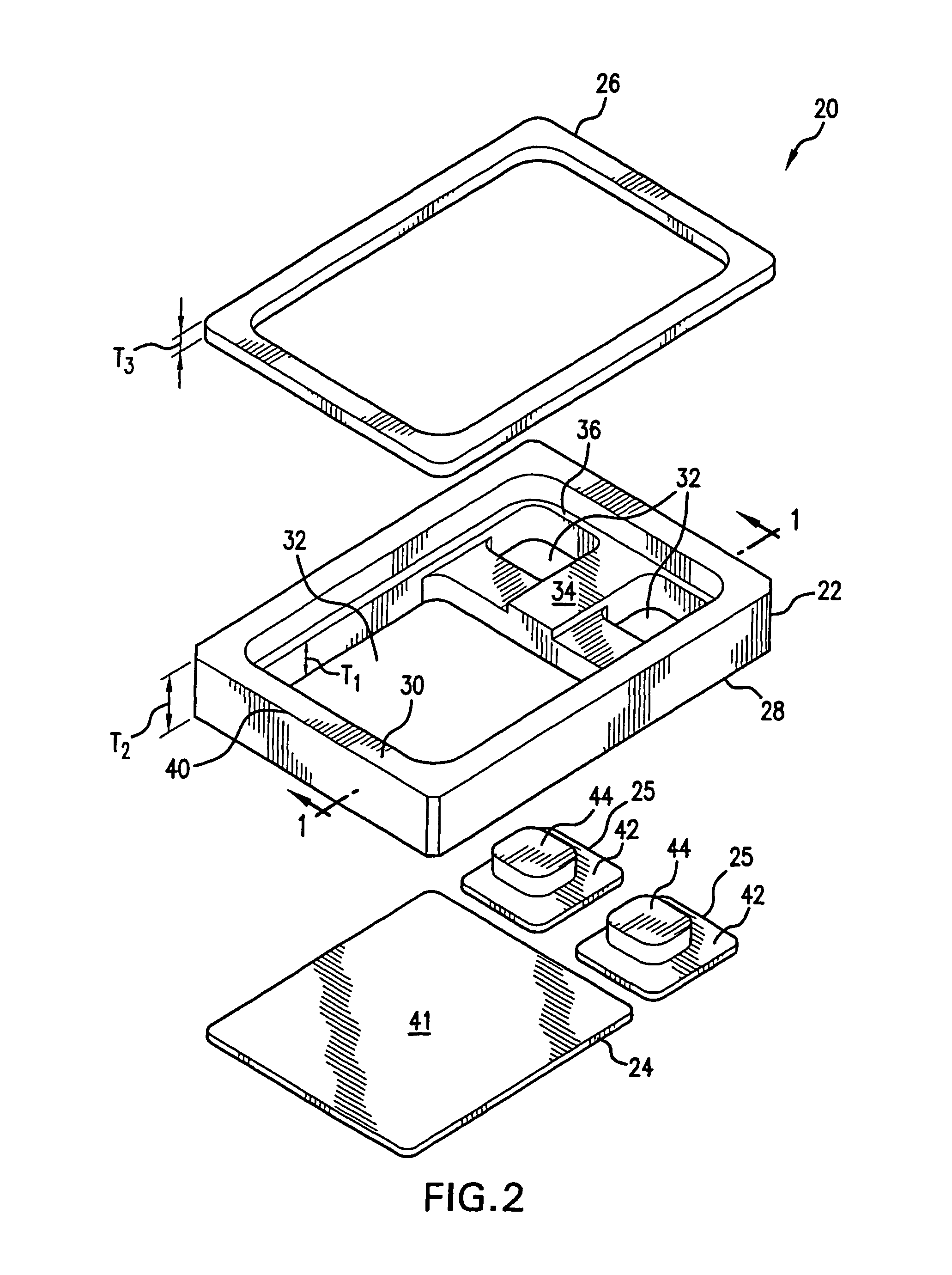
[0029]Generally, the disclosed subject matter relates to a package for housing an electronic circuit. As shown in FIGS. 1 and 2, some embodiments include a package 20 for use in encapsulating an electronic device, such as a semiconductor based integrated circuit or a hybrid circuit having both semiconductor devices and passive devices. Package 20 typically includes a dielectric frame 22, an electrically conductive chip attach pad 24, one or more electrically conductive wire bonding pedestals 25, and a seam weldable, low-profile metallic seal ring 26, all of which are bonded together.

[0030]Dielectric frame 22 includes first and second sides, 28 and 30, respectively, an aperture or apertures 32, and a raised shelf portion 34 defined along an internal perimeter 36 of the dielectric frame and extending outwardly from the second side, and a raised sidewall 38 extending outwardly from the second side along an external perimeter 40 of the dielectric frame. Raised shelf portion 34 defines a...


PUM


Abstract

A package for use in encapsulating an electronic device is disclosed. The package includes a dielectric frame having first and second sides with a pair of apertures extending through the dielectric frame. These apertures are separated by a raised shelf span extending inwardly from an internal perimeter of the dielectric frame. The raised shelf span defines a first thickness of the dielectric frame and a raised sidewall extending outwardly from the second side along an external perimeter of said dielectric frame defines a second thickness of said frame, with the second thickness being greater than the first thickness. Also provided is a metallic component having a flange and a pedestal that extends perpendicularly from the flange. The flange is bonded to the first side of the dielectric frame and extends across one of the pair of apertures with the pedestal extending into that aperture. A gap between the pedestal and the dielectric frame having a width of at least 0.015 inch. This prevents debris from being trapped in the gap and minimizes a risk of particle impact noise detection (PIND) failure.

Description

CROSS REFERENCE TO RELATED APPLICATION(S)[0001]This patent application is a continuation-in-part of U.S. patent application Ser. No. 12 / 456,412, now U.S. Pat. No. 8,080,872, that was filed on Jun. 16, 2009 and is titled “Surface Mount Package with High Thermal Conductivity”. U.S. patent application Ser. No. 12 / 456,412 relates to and claims priority to U.S. Patent Application Ser. No. 61 / 061,887 titled “Surface Mount Device with High Thermal Conductivity” that was filed on Jun. 16, 2008. Both U.S. patent application Ser. No. 12 / 456,412 and U.S. Provisional Patent Application Ser. No. 61 / 061,887 are incorporated by reference in their entireties herein.U.S. GOVERNMENT RIGHTS[0002]N.A.BACKGROUND[0003]1. Field of the Invention[0004]The disclosed subject matter relates generally to a package for housing an electronic circuit. More particularly, the disclosed subject matter relates to a surface mount package having a composite metal base supported by a dielectric frame with raised sidewall...

Claims


Application Information

Patent Timeline
Patent Type & Authority Patents(United States)
IPC IPC(8): H01L23/34H01L23/10
CPCH01L23/055H01L2924/01079H01L2924/09701H01L2924/0002H01L2924/00
Inventor MEDEIROS, III, MANUEL
Owner HCC AEGIS
Why Eureka
Try Eureka