Flat panel display screen operable for touch position determination system and methods

a flat panel display and position determination technology, applied in the field of touch screen technology, can solve the problems of insufficient frequency to achieve the high sampling rate necessary for position sensing of large modern displays with rapidly changing images, and affecting the image quality of large displays. achieve the effect of integrating touch sensitivity, reducing power consumption, and enabling touch sensitive features

Inactive Publication Date: 2012-03-27
KONICEK JEFFREY C
View PDF107 Cites 25 Cited by
  • Summary
  • Abstract
  • Description
  • Claims
  • Application Information

AI Technical Summary

Benefits of technology

[0028]It is an object of the invention to provide a touch sensitive screen that can be manufactured with only minor modification to existing display technology.
[0034]It is an object of the invention to provide improved systems and methods for enabling touch sensitive features on current display panels with minimal expense and change in design, and that is applicable to a wide variety of flat panel displays including: liquid crystal displays (LCD and LCD-like), organic light-emitting diode displays (OLED), electronic paper, polymer light emitting diode (PLED), and quantum dot displays.
[0036]The above and other objects are also achieved by a system and method that adds touch sensitivity to existing LCD and similar displays with only minor structural modification thereto. For example, according to one aspect of the invention, when the surface of an LCD (or similar) display is touched, the underlying liquid crystal layer is slightly compressed. The pressure of the touch brings the transparent common electrical plane in closer proximity to the pixel plates thus raising the pixel capacitance in the area of compression. This increase in capacitance at the point of contact, when observed, gives an indication of the location of contact. Preferably, during the course of refreshing the screen, or alternatively, at other times desired, each pixel capacitor has its capacitance observed. An observed pixel capacitance higher than a predicted level indicates an area of probable screen depression and a likely area of screen contact by external force such as a finger or stylus. Since the pixels are laid in a tight matrix fashion, the area of screen contact can easily and quickly be determined from knowledge of which pixels are yielding higher observed capacitances.

Problems solved by technology

This then causes the emissive material to illuminate.
However, measuring the charge imparted to such a small capacitance is cumbersome and susceptible to large measurement errors and may require display pixels to be disabled from their primary purpose (that of display) so that the time required to impart a known amount of charge to the pixel can be determined.
However, this reference does not teach how the impedance measurement is to be made, or that there is any beneficial time at which the impedance measurement or comparison should be performed, or further, that there is a frequency preferred for the impedance measurement, etc.
This is effectively a low frequency AC signal and while it may be used to measure impedances, it is not of sufficiently high frequency to achieve a high sampling rate necessary for position sensing of large modern displays with rapidly changing images.
If the measurement is made too long after the change occurs it can be missed.
Additionally, if the object remains in pressure contact with the display screen (i.e., continually touching), its continual contact may not be sensed (owing to there being no ‘change’ or delta to detect).
Another problem with the method is that the high frequency AC is continually applied to the electrode that is common to all display elements and it shares its signal return with the display control circuitry.
This current wastes energy and creates an electrically noisy operating state for the display electronics.
In addition, owing to dielectric losses, the dielectric layer (i.e., the liquid crystal) will heat up which could shorten its life significantly.
Application of a touch sensitive technology and associated electronics to an LCD display, for the purpose of manufacturing a touch sensitive display panel, has in the past involved added cost and steps and increased the thickness of the display panel with applied films or extra panels or conductors (which usually dim the display as well).

Method used


Image

  • Flat panel display screen operable for touch position determination system and methods
  • Flat panel display screen operable for touch position determination system and methods
  • Flat panel display screen operable for touch position determination system and methods

Examples


Embodiment Construction

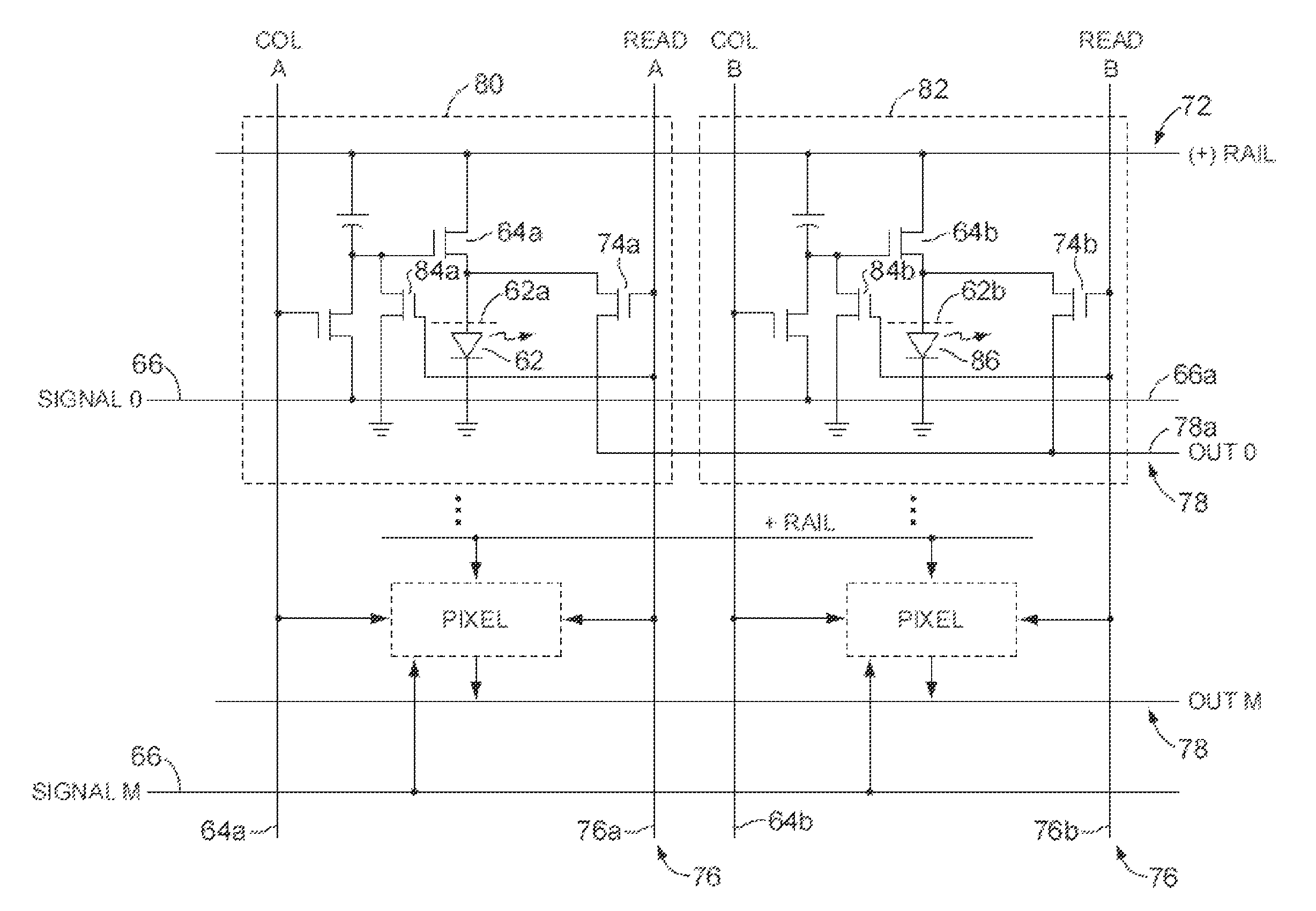
[0050]In the following description, for the purposes of explanation, numerous specific details are set forth in order to provide a thorough understanding of the various aspects of the present invention. It will be obvious, however, to one skilled in the art that the present invention may be practiced without these specific details. In other instances, well known structures and devices are shown or discussed generally in order to avoid obscuring the present invention or making the specification unnecessarily long. In that regard, in order to further shorten the specification, numerous existing patents and publications are discussed and incorporated by reference above and below. It should be noted that there exist many different display system configurations and technologies to which the present invention may be applied and that, while exemplary preferred embodiments are used to illustrate and explain the various aspects of the invention, application of the various aspect of the inven...


PUM


Abstract

A system and method are disclosed that determines the location of an object touching a display screen. The system and method modifies already existing display technology, including using the underlying structure of many types of existing displays as the touch detecting structure. The systems and methods are applicable to virtually all LCD and LCD-like displays, including emissive displays (OLED, PLED, quantum dot displays, etc.), electronic paper, and others.

Description

BACKGROUND OF THE INVENTION[0001]1) Field of the Invention[0002]The present invention relates to touch screen technology and, more particularly, to a system and method that provides touch sensitivity to existing display panel technology while requiring fewer manufacturing steps, utilizing much of the existing display structure and resulting in reduced cost and a thinner overall panel assembly compared to existing touch sensitive display panels.[0003]2) Description of the Art[0004]Modem LCD display technology is well known in the art. Briefly, Liquid Crystal Display (LCD) technology uses two clear panels which orthogonally polarize light. Sandwiched between the panels is a layer of liquid crystal material which can change the polarized direction of light. In quiescent state, and assuming twist nematic (TN) liquid crystal, the panel appears clear since the relaxed liquid crystal twists the polarization vector of the light from one polarized panel through 90 degrees to match the other ...

Claims


Application Information

Patent Timeline
Patent Type & Authority Patents(United States)
IPC IPC(8): G09G3/36G06F3/045
CPCG06F3/0412G06F3/0444G06F3/04184G06F3/0443G06F3/04166G06V40/12G06F3/044G06F2203/04103G06F2203/04101G06F2203/04105G06F2203/04111
Inventor KONICEK, JEFFREY C.
Owner KONICEK JEFFREY C
Why Eureka
Try Eureka