Stress sensor and assembly method thereof

a stress sensor and sensor technology, applied in the direction of mechanical measuring arrangement, instruments, mechanical means, etc., can solve the problems of reducing assembly efficiency, reducing assembly efficiency, and increasing the overall height and overall weight of the electronic device, so as to achieve compact size and low cost , the effect of increasing assembly efficiency

Inactive Publication Date: 2012-04-03
ELAN MICROELECTRONICS CORPORATION
View PDF9 Cites 6 Cited by
  • Summary
  • Abstract
  • Description
  • Claims
  • Application Information

AI Technical Summary

Benefits of technology

[0009]The present invention provides a stress sensor with compact size and low cost.
[0010]The present invention further provides an assembly method for raising the assembly efficiency.
[0016]The fixing effect and degree of fixing the circuit board to the metallic back plane using fixing material such as solder, silver paste or other heat-solidified materials are increased by forming the fixing material coating region. Therefore, the stress sensor of the present invention has compact size and low cost due to less amounts of elements, and the assembly efficiency is increased due to the step simplification resulted from fixing the circuit board to the metallic back plane.

Problems solved by technology

Therefore, when the conventional stress sensor is attached onto a structure such as keyboard body of an electronic device by fastening screws through the fastening holes 163 of the fixing element 15, the overall height and the overall weight of the electronic device are increased and thus the electronic device can not achieve advantages of small in size and light weight.
In addition, the larger amounts of the elements of the conventional stress sensor reduce the assembly efficiency and increase the cost.

Method used


Image

  • Stress sensor and assembly method thereof
  • Stress sensor and assembly method thereof
  • Stress sensor and assembly method thereof

Examples


Embodiment Construction

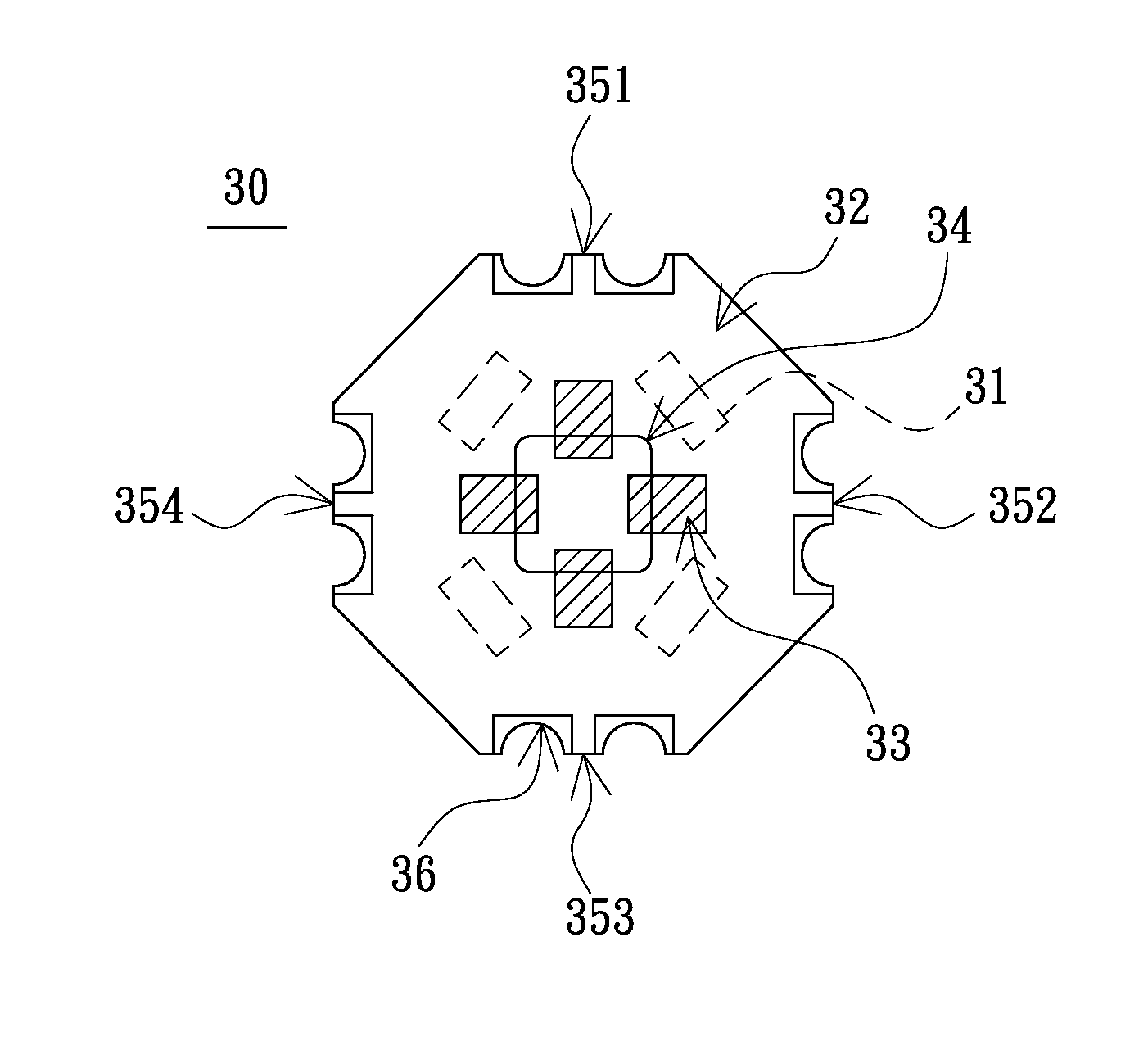
[0028]In an embodiment, the stress sensor used as a pointing device of an electronic device includes a circuit board, a pointing stick and a metallic back plate. As shown in FIG. 3A, an octagonal circuit board 30 has a top (not shown), a bottom 32 and a stress sensitive structure. The top of the circuit board 30 has several junction parts 31 for connecting to the corresponding junction parts 521 (illustrated in FIG. 4C) of a signal cable. The stress sensitive structure includes a stress deformation region (not shown) and several resistors 33. It's noted that the octagonal circuit board 30 has larger contacting area than that of circular circuit board or rectangular circuit board. However, the shape of the circuit board 30 is not to be limited by the illustrated embodiments. In addition, the electronic device can be a notebook computer, a mouse, a keyboard, a hand-held device or a joystick that can equip the stress sensor.

[0029]Moreover, the pointing stick 34 is disposed on the top o...


PUM

PropertyMeasurementUnit
stress sensitiveaaaaaaaaaa
metallicaaaaaaaaaa
stress deformationaaaaaaaaaa

Abstract

A stress sensor includes a circuit board having a stress sensitive structure, a pointing stick and a metallic back plate. The stress sensitive structure includes a stress deformation region and multiple resistors located on the stress deformation region. The pointing stick is disposed on a top of the circuit board and connected to the stress sensitive structure. The metallic back plate includes at least one fixing material coating region, and thus the fixing edges of the circuit board are fixed on the corresponding fixing material coating region. An assembly method for the stress sensor is also provided.

Description

[0001]This application is based upon and claims the benefit of priority from the prior Taiwanese Patent Application No. 098122236, filed Jul. 1, 2009, the entire contents of which are incorporated herein by reference.BACKGROUND[0002]1. Field of the Invention[0003]The present invention relates to a sensor and an assembly method, and more particularly, to a stress sensor fixing to an electronic device and an assembly method thereof.[0004]2. Description of the Related Art[0005]The stress sensor adapted to be used as pointing device is widely used in many types of electronic devices such as laptop, mouse device, keyboard, hand-held device, joystick and the like. For example, the common stress sensor of a laptop is arranged among keys of the keyboard. When a user touches the stress sensor with a finger, the stress sensor senses the magnitude and the direction of the force exerted by the user and then a corresponding movement of cursor is performed.[0006]FIGS. 1A and 1B are schematic thre...

Claims


Application Information

Patent Timeline
Patent Type & Authority Patents(United States)
IPC IPC(8): G01L1/00G06F3/0338
CPCG01B7/18G06F3/0338Y10T29/49826
Inventor LIN, CHUN-HUAKARASAWA, FUMIAKIHUANG, CHUN-CHIEHHUANG, SHIH-LANG
Owner ELAN MICROELECTRONICS CORPORATION
Why Eureka
Try Eureka