Chip pad resistant to antenna effect and method

a chip pad and antenna effect technology, applied in the direction of electrical equipment, semiconductor devices, semiconductor/solid-state device details, etc., can solve the problems of reducing the strength of the gate oxide, affecting the performance of the gate poly electrode, etc., to achieve the effect of being resistant or immune to the antenna

Inactive Publication Date: 2012-04-03
TAIWAN SEMICON MFG CO LTD
View PDF8 Cites 10 Cited by
  • Summary
  • Abstract
  • Description
  • Claims
  • Application Information

AI Technical Summary

Problems solved by technology

The resulting voltage on the gate poly electrode may become so large that charges may flow into the gate oxide, become trapped in the gate oxide or flow through the gate oxide.
These charges may significantly degrade the gate oxide strength and cause MOS device reliability failures.
A small gate oxide region connected to a large poly geometry or a large interconnect metal geometry through poly contacts can accumulate a disproportionate amount of charges (positive plasma ions in the case of a grounded or a negative biased wafer) and may suffer serious damage.
Although being effective in interconnect metal layers, the diode-dropping and the metal jumper scheme described above are less effective in preventing antenna effect associated with chip pads on an IC for at least the following reasons.
First, the diode drop scheme may require changing the original circuit topology in an IC, thus affecting circuit performance.
Second, the bonding surface of a chip pad is typically formed in the uppermost conductive pad layer, therefore forming metal jumpers from thereon is not feasible.

Method used


Image

  • Chip pad resistant to antenna effect and method
  • Chip pad resistant to antenna effect and method
  • Chip pad resistant to antenna effect and method

Examples


Embodiment Construction

[0023]The making and using of the presently preferred embodiments are discussed in detail below. It should be appreciated, however, that the present invention provides many applicable inventive concepts that can be embodied in a wide variety of specific contexts. The specific embodiments discussed are merely illustrative of specific ways to make and use the invention, and do not limit the scope of the invention.

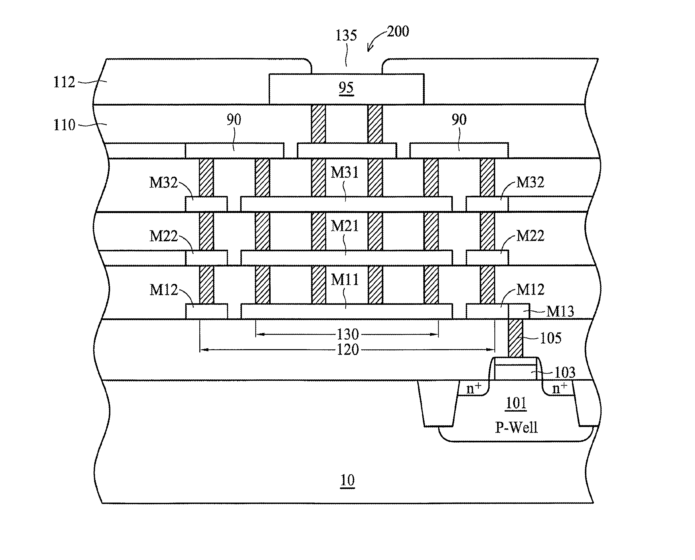
[0024]The present invention will be described with respect to preferred embodiments in a specific context, namely chip pad structures and methods resistant to antenna effect. The preferred embodiments may be used as probe pads on a parametric testline that is typically formed in an area between adjacent IC dies on a wafer and used to measure the electrical characteristics of the devices formed in an IC. The preferred embodiments may also be used as bonding pads on an IC that are bonded by metal wires to make electrical connections to an IC package. The antenna-effect-resistan...


PUM


Abstract

A chip pad structure of an integrated circuit (IC) and the method of forming are disclosed. The chip pad comprises a main pad portion and a ring pad portion. During a charging process involved in forming the chip pad structure, electrical connections from the gate electrodes of MOS transistors in the IC substrate generally are made only to the ring pad portion that has an antenna-to-gate area ratio substantially below a predetermined antenna design rule ratio, and thus is resistant or immune to antenna effect. The main pad portion and the ring pad portion are coupled together through metal bridges formed in an upper interconnect metal layer or in the top conductive pad layer. The chip pad may be used as probe pads on a parametric testline or bonding pads on an IC.

Description

TECHNICAL FIELD[0001]The present invention relates generally to the manufacture of integrated circuits, and more particularly to the structure of an antenna-effect-resistant chip pad in an integrated circuit, and methods of fabricating the same.BACKGROUND[0002]In the manufacturing of an integrated circuit (IC) using Metal-Oxide-Semiconductor (MOS) technology, processes involving charged ions are typically employed, such as a plasma etching process and an ion implantation process. As an example, during a plasma etching process used in forming gate polysilicon (poly) patterns or interconnect metal line patterns, electrostatic charges may accumulate on a floating gate poly electrode. The resulting voltage on the gate poly electrode may become so large that charges may flow into the gate oxide, become trapped in the gate oxide or flow through the gate oxide. These charges may significantly degrade the gate oxide strength and cause MOS device reliability failures.[0003]Each poly gate reg...

Claims


Application Information

Patent Timeline
Patent Type & Authority Patents(United States)
IPC IPC(8): H01L23/52
CPCH01L21/76838H01L24/03H01L23/481H01L23/48H01L24/05H01L2924/13091H01L2924/00014H01L2224/05553H01L2224/02122H01L2924/01033H01L2924/01006H01L2924/30105H01L2924/14H01L2924/05042H01L2224/05093H01L2224/05096H01L2224/05552H01L2224/05624H01L2224/05647H01L2224/451H01L2924/01005H01L2924/01013H01L2924/01014H01L2924/01015H01L2924/01025H01L2924/01029H01L2924/01061H01L2924/01074H01L2924/00012H01L2224/48H01L2924/00H01L2224/02166
Inventor WENG, WU-TENIEH, JI-SHYANG
Owner TAIWAN SEMICON MFG CO LTD
Why Eureka
Try Eureka