
Low noise receiving apparatus

a low noise, receiving apparatus technology, applied in low noise amplifiers, gated amplifiers, high frequency amplifiers, etc., can solve the problems of increasing the chip area and chip cost, increasing the circuit size and cost, and increasing the chip area. , to achieve the effect of reducing the number of output matching circuits, reducing the loss of bypass signals, and low nois

Inactive Publication Date: 2012-04-03
RENESAS ELECTRONICS CORP
View PDF7 Cites 8 Cited by
  • Summary
  • Abstract
  • Description
  • Claims
  • Application Information

AI Technical Summary

Benefits of technology

The present invention is a low noise receiving apparatus that has an amplifier, an output matching circuit, a bypass circuit, and a switching circuit. The apparatus can switch between an amplification mode and a bypass mode. In the amplification mode, the switch circuit connects the output of the amplifier to the output matching circuit, while in the bypass mode, the switch circuit connects the output of the amplifier to the alternating current ground. This switching circuit allows for impedance matching between the output of the amplifier and the output matching circuit in both modes. The apparatus reduces the number of output matching circuits and also reduces the loss of the bypass signal in the bypass mode.

Problems solved by technology

Therefore, the apparatus disclosed in Japanese Unexamined Patent Application Publication No. 10-84300 requires more devices and generates problems such as increasing the circuit size and cost.
Further, the capacitor or the inductor used for the matching circuit generally has large circuit size.
This generates problems of increasing the chip area and also the chip cost.
Therefore, the inventor has found a problem that when passing through the bypass circuit 83, an inconsistency is generated in the impedance of the output matching circuit 87, and the loss of the bypass signal becomes larger.

Method used


Image

  • Low noise receiving apparatus
  • Low noise receiving apparatus
  • Low noise receiving apparatus

Examples


Embodiment Construction

[0024]The invention will now be described herein with reference to illustrative embodiments. Those skilled in the art will recognize that many alternative embodiments can be accomplished using the teachings of the present invention and that the invention is not limited to the embodiments illustrated for explanatory purposes.

[0025]Hereafter, an embodiment of the invention is described with reference to the drawings.

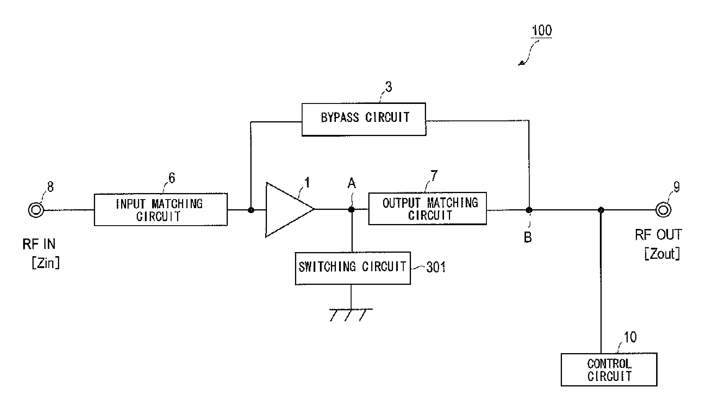
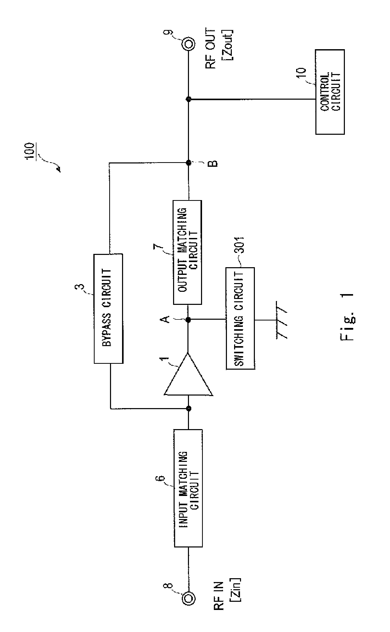
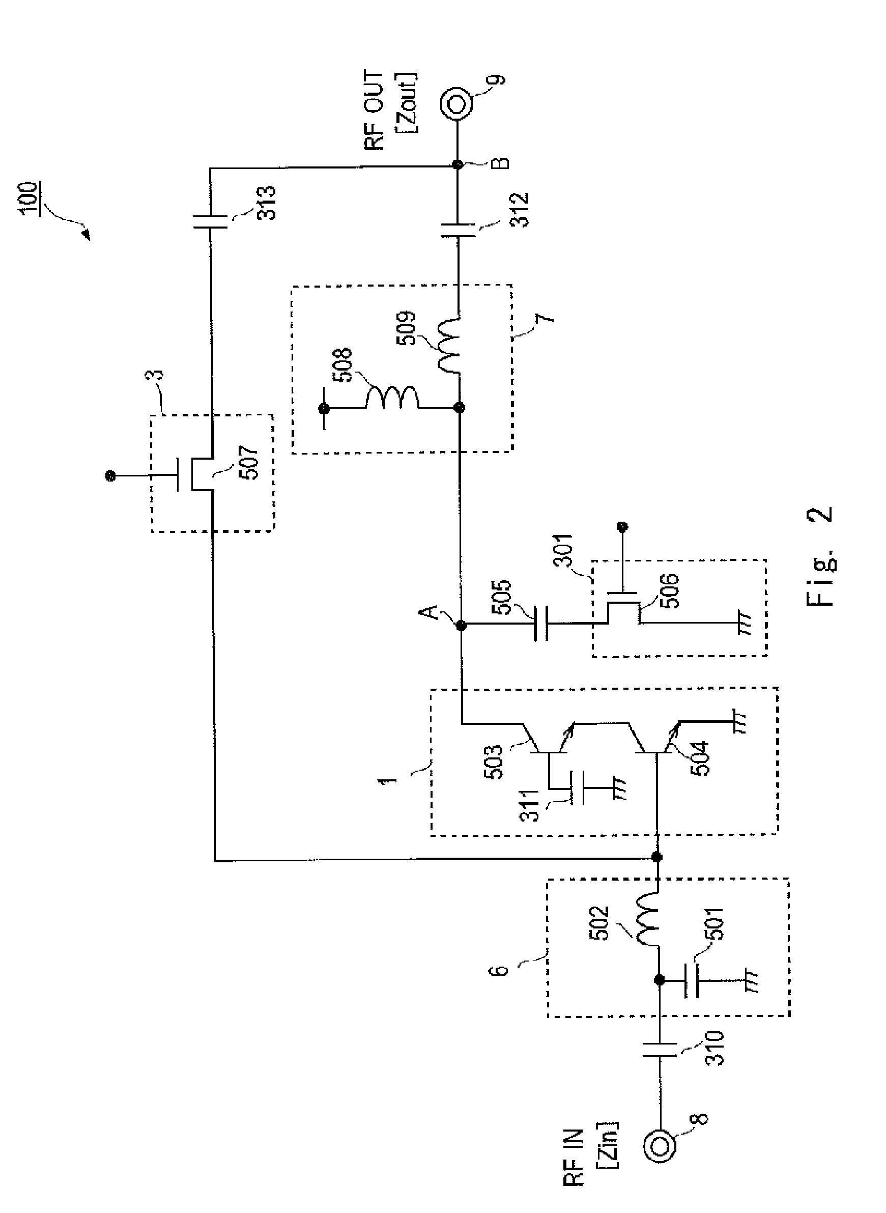
[0026]FIG. 1 is a block diagram illustrating a configuration example of a low noise receiving apparatus according to the exemplary embodiment of the present invention. A low noise receiving apparatus 100 includes an amplifier 1 for amplifying an input signal RF_IN, an output matching circuit 7 connected between the amplifier 1 and an output terminal 9 for matching an impedance of the output side of the amplifier 1, a bypass circuit 3 having its output connected to the output side of the output matching circuit 7 for bypassing the amplifier 1, and a switching circuit 301 ha...


PUM


Abstract

A low noise receiving apparatus includes an amplifier which inputs an input signal, an output matching circuit which is connected between the amplifier and an output terminal which matches an impedance of an output side of the amplifier, a bypass circuit which bypasses the amplifier and is connected to an output side of the output matching circuit, and a switching circuit having one end connected between the amplifier and the output matching circuit and the other end connected to an alternating current ground which switches whether or not to connect an output of the amplifier to the alternating current ground. In a bypass mode, the switching circuit connects the output of the amplifier to the alternating current ground in order to have a lower impedance viewed from the output terminal of the output matching circuit than in an amplification mode.

Description

BACKGROUND OF THE INVENTION[0001]1. Field of the Invention[0002]The present invention relates to a low noise receiving apparatus provided in a high-frequency front-end circuit, and particularly to a low noise receiving apparatus which switches an amplification operation and a bypass operation depending on an input RF (Radio Frequency) signal strength. The amplification operation is to amplify the input RF signal by an amplifier, and the bypass operation is to bypass the amplifier.[0003]2. Description of Related Art[0004]In recent years, mobile terminals such as Wireless-LAN (Local Area Network), D-TV (Digital Television), and GPS (Global Positioning System) are increasing rapidly. In a low noise receiving apparatus mounted to such mobile terminal, generally an amplifier to amplify an RF signal is provided in a front-end circuit in order to obtain a good receive sensitivity. The mobile terminals can be used at any place without limitation, and low noise receiving apparatuses need to ...

Claims


Application Information

Patent Timeline
Patent Type & Authority Patents(United States)
IPC IPC(8): H03F1/14H03F3/04
CPCH03F1/22H03F3/19H03F3/72H03G1/0088H04B1/18H03F2200/294H03F2200/451H03F2203/7239H04B1/16H04B1/10
Inventor TAKEUCHI, TOMOHIKO
Owner RENESAS ELECTRONICS CORP
Learn More