Method for manufacturing printed wiring board

Active Publication Date: 2012-04-17
IBIDEN CO LTD
View PDF22 Cites 4 Cited by
  • Summary
  • Abstract
  • Description
  • Claims
  • Application Information

AI Technical Summary

Benefits of technology

[0016]A Pd layer (palladium layer) can reduce the chances of a defect occurring such as the eventuality of a repellent solder. Thus, in comparison with a conventional solder pad structure, the degree of adhesiveness with a solder can be further improved.
[0145]Although the present invention is applied to a build-up printed wiring board, and to a subtraction multilayered board, the same effects can be expected when it is applied to various boards such as a single face circuit board, to a double face circuit board, to a flexible board, flexible board in which a reel-to-reel method is used to a ceramic board and to a AIN board.

Problems solved by technology

However, if the diameter of the solder pad is small (for example, the opening diameter of the solder pad is less than 200 μm), when the solder paste is formed on the solder pad by means of printing, the shape of the solder bump, or of the solder layer that connects with the external terminal sometimes cannot be maintained because of a defect such as insufficient charging, or a lack of charging of the solder on the pad, and on occasions functioning as a solder bump, or as a solder layer, becomes impossible.
Consequently, the degree of electric connectivity and reliability may on occasions drop.
Further, as the diameter of the opening of the solder pad decreases, the connecting area between the solder pad and the solder bump may for example, decrease and this may at times result in a deterioration in adhesive property.
Further, bubbles may be formed in the solder paste or in the solder layer, and such bubbles may cause the solder to burst, or bubbles may remain in the solder, and this may on occasions lead to a deterioration in the ability of the solder perform a functions of electric connectivity.
This has resulted in a deterioration in the degree of reliability at an early stage.

Method used


Image

  • Method for manufacturing printed wiring board
  • Method for manufacturing printed wiring board
  • Method for manufacturing printed wiring board

Examples


embodiment 1

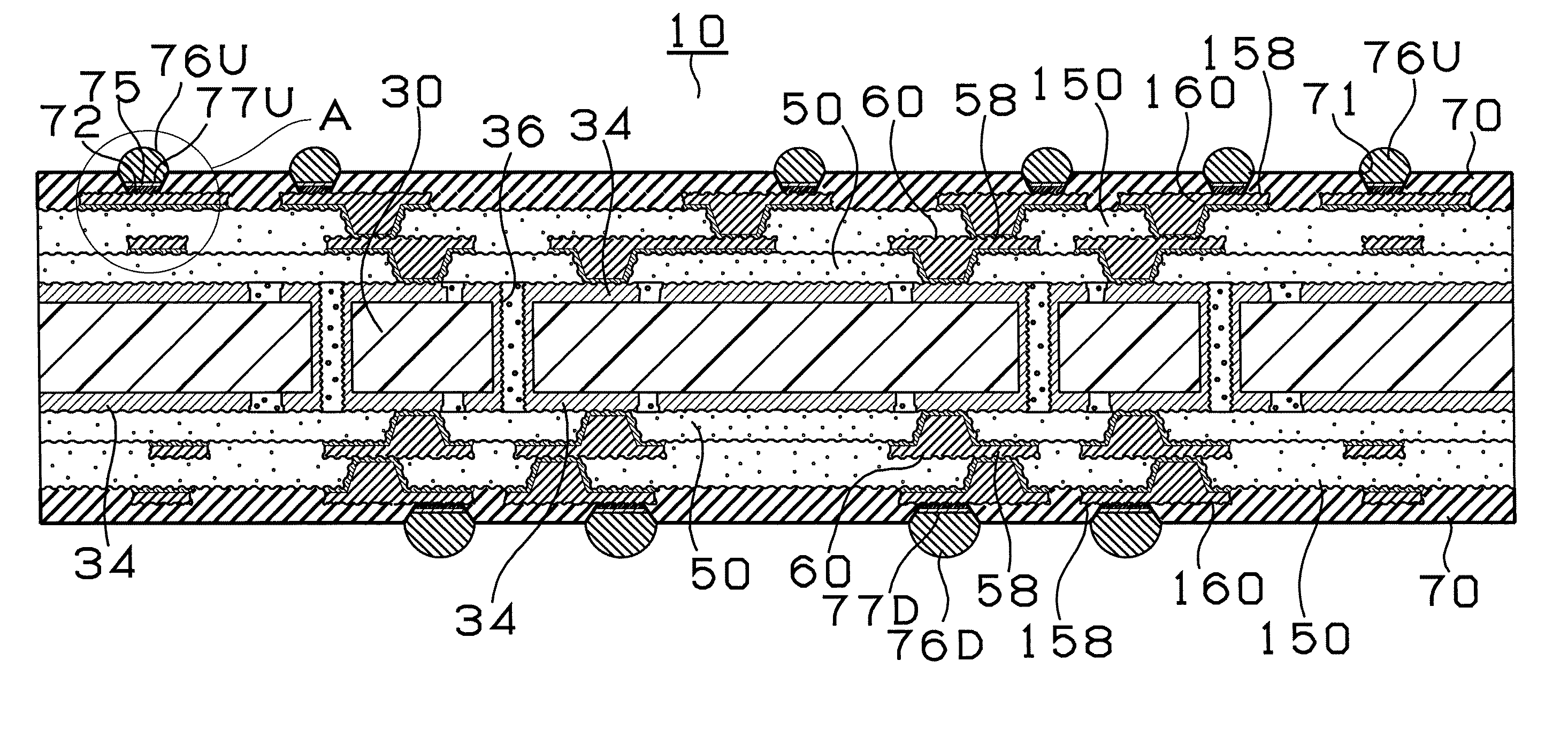
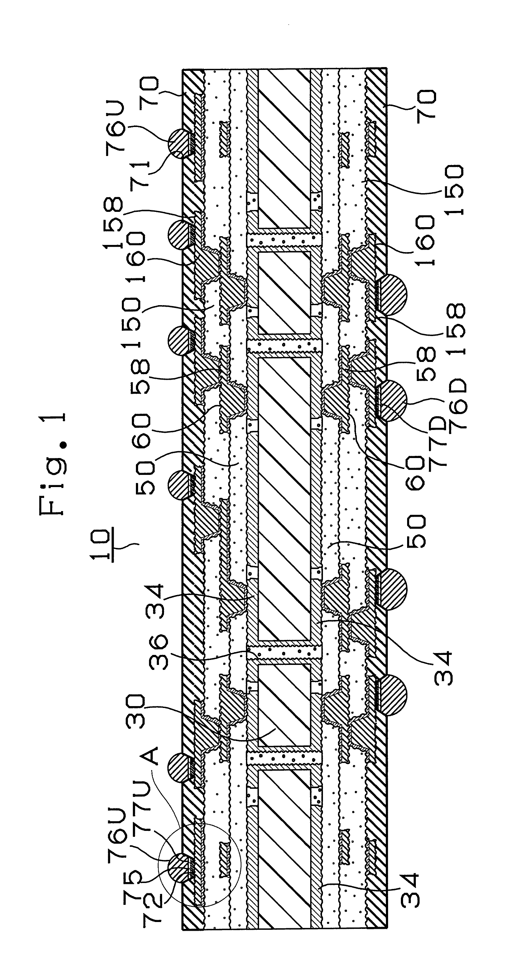
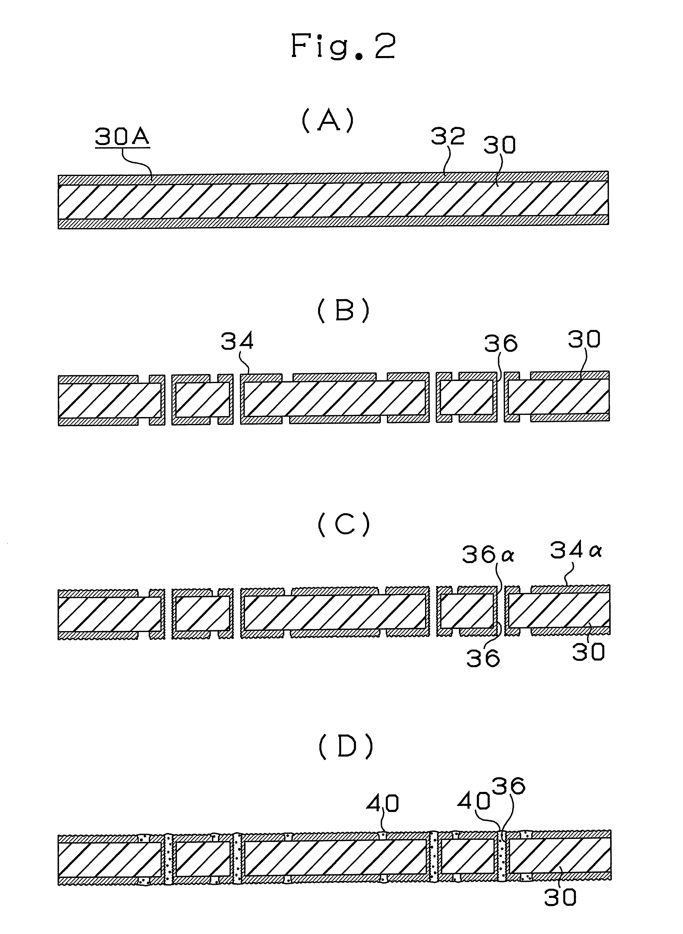
[0216]The configuration of a multilayer printed wiring board 10 according to Embodiment 1 of the present invention will first be described with reference to FIG. 1 showing the cross section thereof. The multilayer printed wiring board 10 has a conductor circuit 34 formed on the front surface of a core substrate 30. The front and rear surfaces of the core substrate 30 are connected to each other via through holes 36. In addition, an interlayer resin insulating layer 50 on which via holes 60 and conductor circuits 58 are formed and an interlayer resin insulating layer 150 on which via holes 160 and conductor circuits 158 are formed are provided on the both surfaces of the core substrate 30. Solder resist layers 70 are formed on upper layers of the via holes 160 and the conductor circuits 158, and solder pads 77U and 77D are formed on the conductor circuits 158 through the opening portions 71 of the solder resist layers 70, respectively. Bumps 76U and 76D are formed on the solder pads ...

embodiment 1-1-1

[0261]In embodiment 1-1-1, an alloy of Cu: 0.5 wt %, Ag: 3.5 wt %, Sn: 95 wt % is used as a solder consisting of the solder bump. Ni layer is formed as thickness 5 μm, P content 1.2 wt %. On the other hand, Pd layer is formed as thickness 0.5 μm, P content 5 wt %. Therefore, the composition of the Ni—Sn alloy layer becomes Sn:Cu:Ni=42:37:21, the thickness becomes 1.5 μm. Electron microscope pictures of Ni layer, Cu—Ni—Sn alloy and solder in embodiment 1-1-1 are shown in FIGS. 15-18. The electron microscope picture (×20 k) in the left side of FIG. 15 shows embodiment 1-1-1. The electron microscope pictures (×100 k) in the left sides of FIGS. 16, 17 are a more enlarged scale. The right sides of electron microscope pictures in FIGS. 15, 16, 17 show Pd layers which do not contain P in reference example 1-1-1. The lower side is the Ni layer and the upper side is the solder and the interface between the Ni layer and the solder is the Cu—Ni—Sn alloy. As shown in the electron microscope pic...

embodiment 1-1-2

[0262]In embodiment 1-1-2, an alloy of Cu: 0.5 wt %, Ag: 3.5 wt %, Sn: 95 wt % is used as a solder consisting of the solder bump. Ni layer is formed as thickness 5 μm, P content 1.2 wt %. On the other hand, Pd layer is formed as thickness 0.01 μm, P content 2 wt %. Therefore, the composition of the Ni—Sn alloy layer becomes Sn:Cu:Ni=42:37:21, the thickness becomes 1.8 μm. The Ni—Sn alloy layer is typically a board-shaped form.


PUM

PropertyMeasurementUnit
Thicknessaaaaaaaaaa
Thicknessaaaaaaaaaa
Thicknessaaaaaaaaaa

Abstract

A composite layer composed of an Ni layer and a Pd layer is formed on a solder pad, and a solder on the composite layer is composed of a solder containing no lead. Because a Pd layer (palladium layer) reduces phenomenons such as repellency of the solder, adhesiveness with the solder can be enhanced. Because a Pd layer has a higher degree of rigidity than a gold layer, thermal stress is absorbed into the Pd layer and buffered so as to reduce the degree of transmission of stress to the solder bump, or to the solder layer, by thermal stress.

Description

CROSS-REFERENCE TO RELATED APPLICATIONS[0001]This application is a divisional of and claims the benefit of priority under 35 U.S.C. §120 from U.S. Ser. No. 11 / 576,987, filed Nov. 12, 2007, the entire contents of this application is incorporated herein by reference. U.S. Ser. No. 11 / 576,987 is a National Stage of PCT application No. PCT / JP05 / 04558, filed Mar. 15, 2005, and claims the benefit of priority under 35 U.S.C. §119 from Japanese Patent Application Nos. 2004-300696, filed Oct. 14, 2004; 2004-300697, filed Oct. 14, 2004; 2004-373471, filed Dec. 24, 2004; and 2004-373472, filed Dec. 24, 2004.TECHNICAL FIELD[0002]The present invention relates to a multilayered printed wiring board for accommodation of a semiconductor, on which a semiconductor device is loaded.BACKGROUND ART[0003]The outermost layer of a printed wiring board generally has a solder resist layer in order to protect a conductor circuit. When a solder bump is to be formed, a solder pad is formed by opening part of th...

Claims


Application Information

Patent Timeline
IPC IPC(8): H01K3/10H01L21/44
CPCH01L21/4853H01L23/49816H05K3/244H01L23/498Y10T29/49156H01L2224/32225H01L2224/48091H01L2224/48227H01L2224/73265H01L2924/01004H01L2924/01012H01L2924/01046H01L2924/01078H01L2924/01079H01L2924/15311H01L2924/19041H05K3/3463H05K3/4644Y10T29/49165Y10T29/4913Y10T29/49126Y10T29/49128Y10T29/49155H01L2924/12041H01L2924/01019H01L24/48H01L2924/00014H01L2924/00012H01L2924/00H01L24/73H01L2224/45099H01L2224/45015H01L2924/207
Inventor IWAI, TSUTOMUKODERA, YOSHIHIROMAEDA, SHINYAWATANABE, HIROYUKISUZUKI, KAZUNARITSUKADA, KIYOTAKA
Owner IBIDEN CO LTD
Why Eureka
Try Eureka