

Method of producing a via in a reconstituted substrate
a substrate and via technology, applied in the field of component integration, can solve the problems of end-of-method testability, difficulty in re-filling, or plugging, and above-mentioned techniques not being able to be don
Active Publication Date: 2012-04-17
COMMISSARIAT A LENERGIE ATOMIQUE ET AUX ENERGIES ALTERNATIVES
View PDF45 Cites 0 Cited by
- Summary
- Abstract
- Description
- Claims
- Application Information
AI Technical Summary
Benefits of technology
The patent text discusses the problem of integrating components in a way that is both compact and cost-effective. The invention proposes a method of producing reconstitutable substrates of components that can be stacked or used in a 3D configuration. The technical effect of this invention is to improve the integration density of electronic systems and reduce the size of components while maintaining their reliability. Other techniques for improving compactness are also discussed in the text.
Problems solved by technology
To achieve this, it is aimed to develop vertical connections inside reconstituted substrates, which the above mentioned techniques do not enable to be done.
This technology has various drawbacks, particularly that of being developed after the positioning of the chips, but also that of being costly: it implements several steps (including 2 lithography steps), and a more or less deep etching in the material; difficulties are also posed of filling, or plugging of the vias by particles created during etching or polishing steps.
Finally, the problem of end of method testability is posed: it is necessary in fact to remove the support and carry out a polishing before being able to test the continuity of the via.
But this technology also poses certain difficulties:a vertical wire 302 needs to be maintained over the whole substrate thickness,there is a limitation in terms of pitch, in other words it is necessary to have available specific tooling to lay the wire 302,a minimum distance between the components and the wires must be respected, on account of the specific tooling for laying the components or wires.
Problems of the precision of positioning the interconnections, the implementation cost (which depends on the number of connections), the end of method testability, the locating of interconnections on the substrate, and the misalignment of the wires with each other are also posed.
But this assembly is made to the detriment of compactness and, moreover, the problem—mentioned above—remains of the interconnections brought back towards the support 215, 217 from the bottom of each stage to avoid the crossing of wires, which implies, once again, a lengthening and an awkward placing of interconnections.
Method used
View moreImage
Smart ImageViewing Examples

Examples
first embodiment
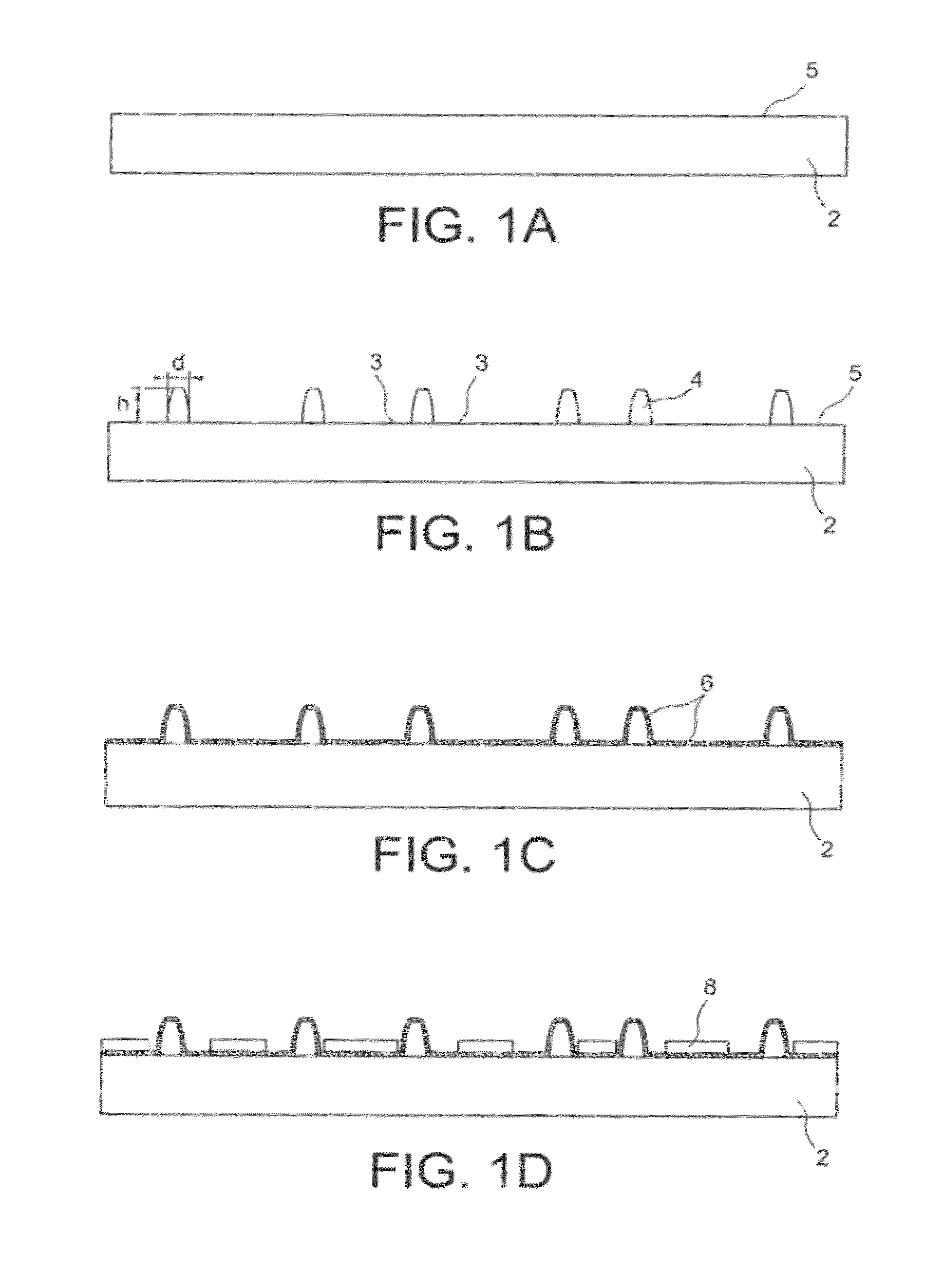
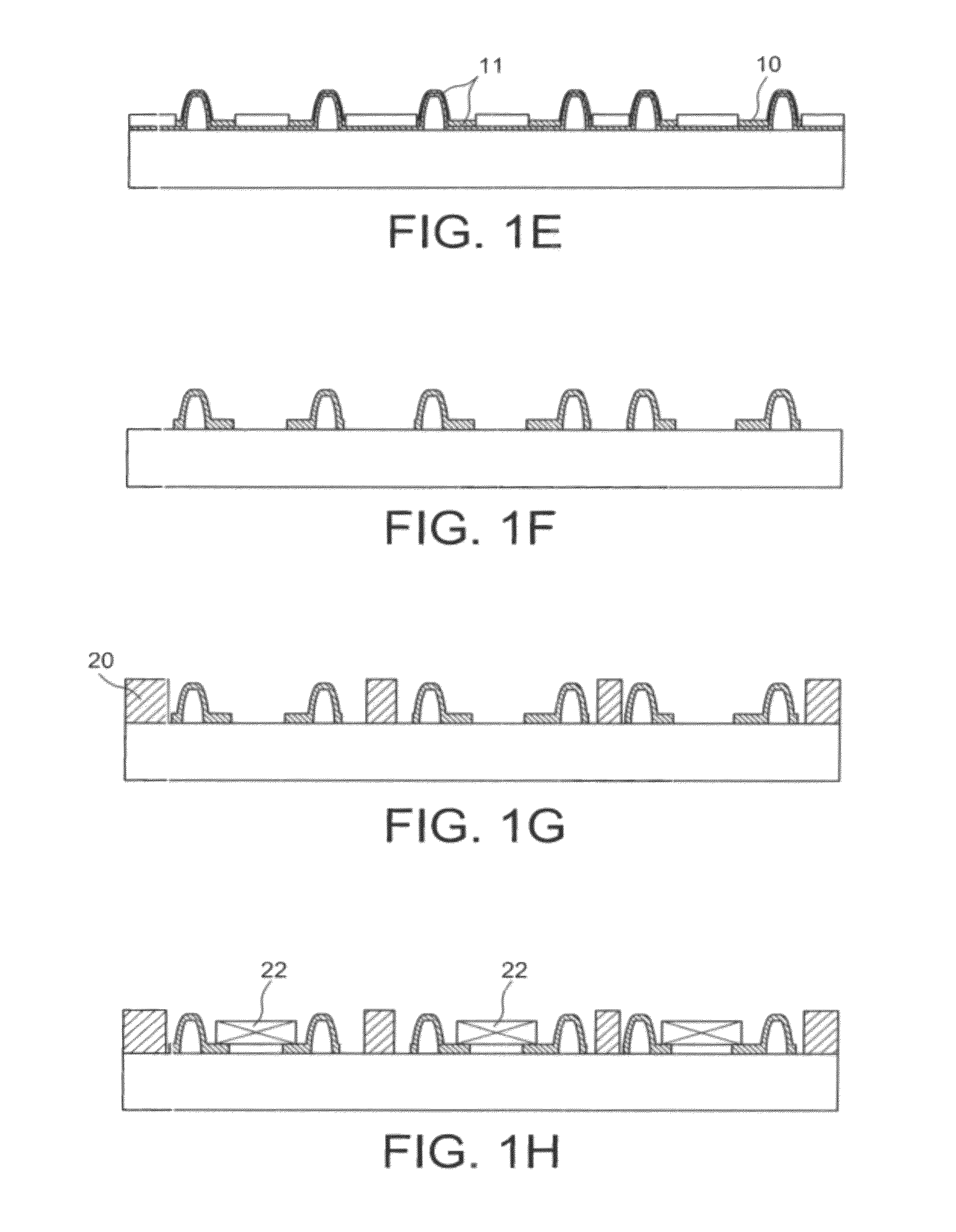
[0051]FIGS. 1A-1J represent a method according to the invention.
second embodiment
[0052]FIGS. 2A-2I represent a method according to the invention.
[0053]FIG. 3 presents examples of polymer pins that may be used within the scope of the present invention.
[0054]FIGS. 4 and 5A-5C represent devices obtained by a method according to the invention.
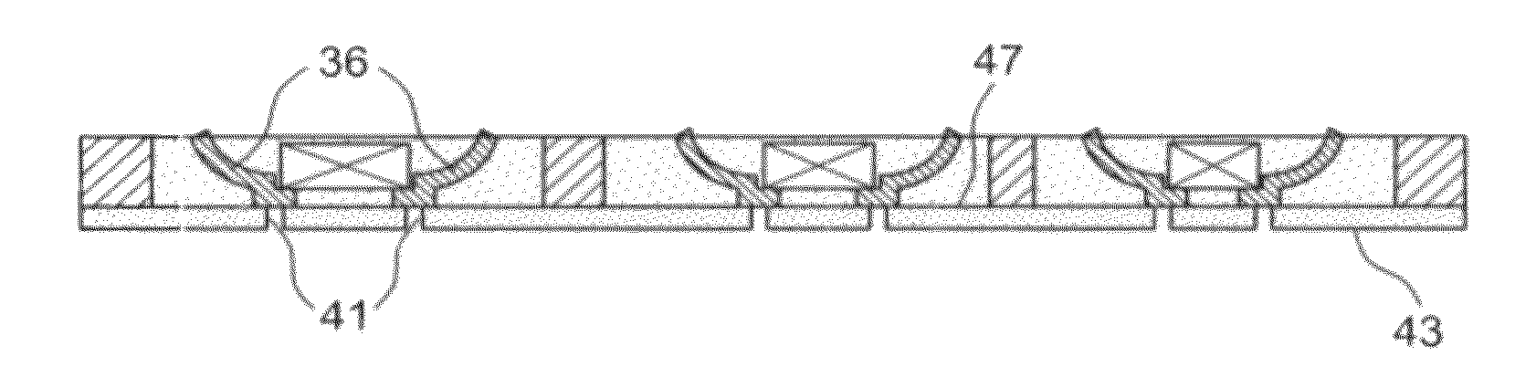
[0055]FIGS. 6A-6C schematically represent various layout examples of a component and vias near to this component.
[0056]FIGS. 7 and 8 represent assemblies of devices obtained by a method according to the invention.
[0057]FIGS. 9, 10, 11A and 11B represent structures known from the prior art.
Login to View More PUM
 Abstract
A method of producing an electronic connection device, including: a) formation, in a plane of a support substrate, of at least one first contact element and, in a direction approximately perpendicular to the plane, of at least one second contact element having a first end in electrical contact with the first contact element or elements and a second end, the second contact element or elements including one or more metal tracks standing up along the direction perpendicular to the surface of the substrate; b) then positioning at least one electrical or electronic component in contact with the first contact element or elements; and c) encapsulation of the component(s) and of the first and second contact elements, at least the second end or ends of the second contact element or elements being flush with the surface of the encapsulating material.
Description
TECHNICAL FIELD AND PRIOR ART[0001]The invention relates to the field of component integration.[0002]It proposes producing integrated component substrates, substrates that in particular contain vertical interconnections and which are suited to the formation of component stackings.[0003]The increase in component integration density and the quest to improve performance and reduce costs lead suppliers of electronic systems to develop more and more compact devices.[0004]Novel integration techniques are known that make it possible to increase the compactness of chips or systems while at the same time reducing their cost and maintaining their reliability.[0005]For instance, document EP 1 596 433 describes the concept of “neo-wafers”, which consists in making a wafer from tested and defined bare chips (cut electronic chips). Elementary technological steps are applied to these substrates to achieve a redistribution of the inputs / outputs of the chips so as to enable final assembly on a PCB (...
Claims
Login to View More Application Information
Patent Timeline
 Patent Type & AuthorityPatents(United States)
IPC IPC(8): H01L29/40
CPCH01L21/568H01L23/5389H01L25/105H01L24/96H01L25/18H01L2225/1035H01L2225/1005H01L2924/1461H01L2224/04105H01L2924/07802H01L2924/00H01L2924/181H01L2924/00012
InventorBALERAS, FRANCOISSOURIAU, JEAN-CHARLESHENRY, DAVID
OwnerCOMMISSARIAT A LENERGIE ATOMIQUE ET AUX ENERGIES ALTERNATIVES