Semiconductor device and method of manufacturing same

a semiconductor and solid-state device technology, applied in the field of semiconductor devices, can solve the problems of high production cost and human labor required to perform this task

Active Publication Date: 2008-09-11
FUJI ELECTRIC CO LTD
View PDF6 Cites 25 Cited by
  • Summary
  • Abstract
  • Description
  • Claims
  • Application Information

AI Technical Summary

Benefits of technology

[0025]In addition, by forming pressing protrusions on the outer face of the terminal clamping frame and pressing these protrusions into the inside of the outer resin case, the terminal clamping frame can be firmly fixed to the outer resin case without looseness.

Problems solved by technology

Moreover, because it is in actuality difficult for an assembly robot to automatically set external terminals 6 with different shapes (see FIGS. 13A and 13B) in specified positions within the forming mold according to the product specifications, human labor is necessary to perform this task.
As a result there is a long period from receipt of an order for a custom product to the delivery of the product, and moreover production costs are high.

Method used


Image

  • Semiconductor device and method of manufacturing same
  • Semiconductor device and method of manufacturing same
  • Semiconductor device and method of manufacturing same

Examples


embodiment 1

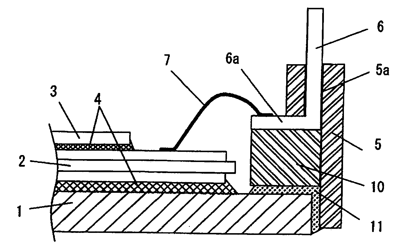
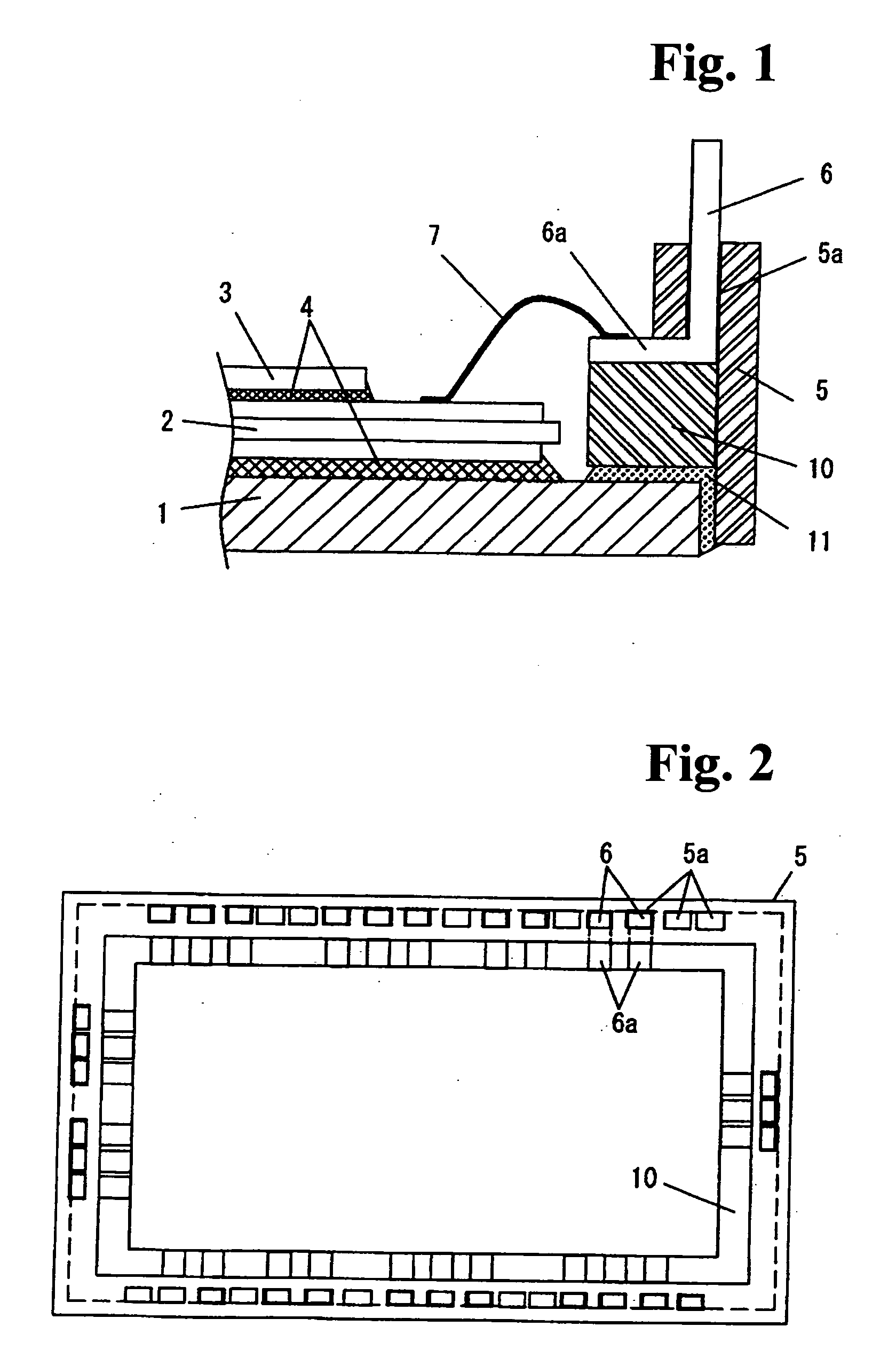
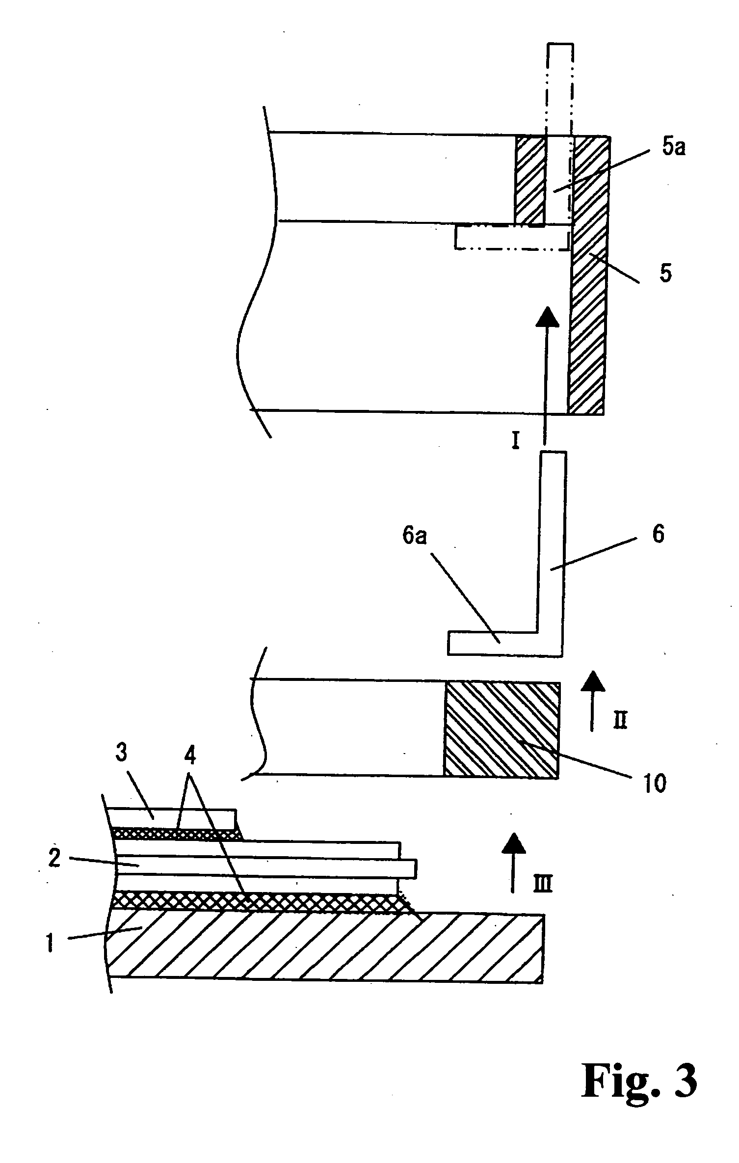
[0040]First, FIG. 1 and FIG. 2 are used to explain the assembled package structure of this embodiment of the invention. This embodiment differs from a structure of the prior art, described in FIG. 11, in which external terminals 6 are insert-molded in an outer resin case 5 in an integral structure with the terminals, in the following respects. That is, in the embodiment shown, terminal mounting holes 5a are formed in advance in a plurality of locations at a fixed pitch interval along the peripheral wall of the outer resin case 5. The terminal mounting holes 5a are formed by casting with cores set in the mold corresponding to the terminal mounting holes in the process of molding the outer resin case 5. Then, at the time of package assembly, holes for mounting of external terminals 6 are selected from the terminal mounting holes 5a according to specifications specified for each device model, and external terminals 6 are pressed thereinto as described below and installed afterwards.

[00...

embodiment 2

[0053]Next, a second embodiment, in which the package structure is further improved on the above Embodiment 1, is explained referring to FIG. 6 through FIG. 10D. In this embodiment, the following structural modifications of the outer resin case 5 and terminal clamping frame 10 are made. That is, depression-protrusion shape step portions 5b are formed along the peripheral wall of the outer resin case 5 on the upper-face side. These depression-protrusion shape step portions 5b are formed at the same pitch as the terminal mounting holes 5a, such that the depression grooves 5b-1 are positioned midway between adjacent terminal mounting holes 5a. By this means, as shown in FIG. 10A, a creepage distance d is formed which is greater than the spatial distance between the external terminals 6 drawn outward from the outer resin case 5, so that a high dielectric strength can be secured.

[0054]On the other hand, pressing protrusions 10a with a cross-sectional V-shape are distributed and formed al...


PUM


Abstract

A semiconductor device includes an outer resin case having a peripheral wall and terminal mounting holes formed in the peripheral wall, and a layer assembly provided in the outer resin case. The layer assembly includes a semiconductor chip, an insulating circuit board on which the semiconductor chip is mounted, and a heat-dissipating metal base. External terminals having leg portions are arranged in mounting holes of the peripheral wall, and are press-fitted into the terminal-mounting holes. Bonding wires connect the terminal leg portions and a conductive pattern of the insulating circuit board or the semiconductor chip.

Description

BACKGROUND OF THE INVENTION AND RELATED ART STATEMENT[0001]This invention relates to a semiconductor device applied in intelligent power modules (IPMs) used in inverter devices, and more specifically relates to the package structure, and the method of assembly of semiconductor devices.[0002]FIG. 11 through FIGS. 13A, 13B show an assembled structure of the semiconductor device packages of the prior art. In FIG. 11, numeral 1 is a heat-dissipating metal base formed from copper; numeral 2 is an insulating circuit board with a conductor pattern formed on both faces of an insulating board; numeral 3 is a semiconductor chip (for example, an IGBT (Insulated Gate Bipolar Transistor)) mounted on the insulating circuit board 2; numeral 4 is solder joining layer, which joins the metal base 1 and insulating circuit board 2, and the insulating circuit board 2 and semiconductor chip 3; numeral 5 is an outer resin case; numeral 6 is an external terminal provided in a row in a wall portion of the o...

Claims


Application Information

Patent Timeline
Patent Type & Authority Applications(United States)
IPC IPC(8): H01L23/48H01L21/52
CPCH01L23/36H01L2924/01013H01L24/45H01L24/48H01L24/85H01L25/072H01L2224/45124H01L2224/48091H01L2224/48472H01L2224/85205H01L2924/13055H01L2924/19107H01L23/49861H01L2224/32225H01L2224/48227H01L2924/1305H01L2224/4911H01L2924/01068H01L2224/73265H01L2924/00014H01L2924/00H01L2924/00012H01L24/73H01L2924/181H01L2924/16195H01L24/49
Inventor YOSHIHARA, KATSUHIKOMARUYAMA, RIKIHIROCHINO, MASAAKIMOCHIZUKI, EIJIYOKOYAMA, MOTOKIYONISHIZAWA, TATSUOSUGIYAMA, TOMONOBU
Owner FUJI ELECTRIC CO LTD
Why Eureka
Try Eureka