Method for manufacturing electrochromic devices

a manufacturing method and electrochromic technology, applied in the field of electrochromic devices, can solve the problems of reducing the lifetime of the device, reducing etc., to achieve high volume and throughput, enhance the manufacturability of the product, and reduce the cost and complexity of the electrochromic device high volume manufacturing

Active Publication Date: 2012-05-01
APPLIED MATERIALS INC
View PDF23 Cites 38 Cited by
  • Summary
  • Abstract
  • Description
  • Claims
  • Application Information

AI Technical Summary

Benefits of technology

[0010]The concepts and methods of the invention allow the cost and complexity of electrochromic device high volume manufacturing to be reduced by eliminating and / or minimizing the use of conventional masks to enhance manufacturability of the products at high volume and throughput and on large area substrates. This can significantly reduce the cost for broad market applicability as well as provide yield improvements. This is achieved while ensuring the active layers of the device are protected over the long term from environmental oxidants. According to aspects of the invention, these and other advantages are achieved with the use of laser patterning / scribing to meet certain or all of the patterning requirements, while integrating the laser scribing so as to ensure the active layers of the device are protected to ensure long term reliability. It is envisaged that the laser is used to pattern the component layers of electrochromic devices by directly removing (ablating) the material of the component layers. As such, this invention contemplates laser patterning integrated into the manufacturing process as deemed appropriate and necessary for electrochromic device manufacturability, yield, functionality, and long term reliability. This includes a manufacturing method for an electrochromic device comprising the following steps: (1) depositing a first transparent conductive layer followed by a cathode on a transparent substrate; (2) patterning the cathode; (3) depositing an electrolyte layer, followed by a counter electrode layer, followed by a second transparent conductive layer; (4) focused laser patterning the electrolyte, counter electrode and transparent conductive layers; (5) depositing a diffusion barrier; and (6) forming separate electrical contacts to the first transparent conductive layer and the second transparent conductive layer. The patterning step in (2) may also be a focused laser patterning process. In this method laser patterning of the first transparent conductive layer and the cathode layer occurs before deposition and laser patterning of the remaining layers, thus eliminating any contamination of the remaining layers due to redeposition of the transparent conductive material and cathode material on their surfaces. Furthermore, during focused laser patterning, ablated material generated by the focused laser patterning may be removed. In general, redeposition of ablated material and particulate contamination due to laser ablation can be minimized by using tactics such as spatially separating edges of upper and lower layers and / or patterning of lower layers prior to deposition of upper layers.

Problems solved by technology

However, exposure of the electrochromic devices to atmospheric oxygen and water can degrade the performance of the devices and reduce the lifetime of the devices.
The use of traditional lithography techniques with physical masks leads to many disadvantages, especially related to high volume manufacturing (HVM).
For example, the use of physical masks: (1) adds a significant capital investment requirement for HVM and large area scaling; (2) increases the cost of ownership (consumable mask cost, cleaning, chemicals, etc.); (3) decreases the throughput because of alignment requirements; and (4) results in a yield loss, since the masks are prone to flaws which translate to defects in the electrochromic devices, such as color centers and pinholes in protective layers.
The presence of pinholes in protective layers will eventually lead to failure of the electrochromic devices due to oxidants reaching the active layers of the devices.
This occurs for electrochromic devices sealed in IGUs when the IGU seal becomes compromised and atmospheric oxidants leak into the unit.
The desired device lifetimes of tens of years cannot be achieved with pinhole defects in the protective layers.
In HVM processes, the use of physical masks (ubiquitous for traditional and current state-of-the-art electrochromic device fabrication technologies) will contribute to higher complexity and higher cost in manufacturing.
The complexity and cost result from the requirement to fabricate very accurate masks and the need to use (automated) management systems for mask alignment and regeneration.
In addition, the higher cost results from the need for maintaining the masks as well as from throughput limitations by the added alignment steps.
The adaptation becomes increasingly more difficult and costly as the manufacturing is scaled to larger area substrates.
Moreover, the scaling (to larger substrates) itself can be limited because of the limited availability and capability of the physical masks.
Furthermore, due to the yield issues associated with mask-based lithography fabrication steps, there remains a need for improved methods for patterning the numerous component layers of electrochromic devices.
However, the laser scribing method of Hichwa et al. results in contamination of the exposed edges of the active electrochromic layers due to redeposition during laser ablation of material on the walls of the trench being cut.
This contamination can impair the performance of the electrochromic device.
When the protective coating is applied, the presence of particulates on the surface can lead to pinholes in the coating.
Pinholes in the protective coating can result in exposure of the device to oxidants from the ambient, and ultimately to premature device failure.

Method used


Image

  • Method for manufacturing electrochromic devices
  • Method for manufacturing electrochromic devices
  • Method for manufacturing electrochromic devices

Examples


first embodiment

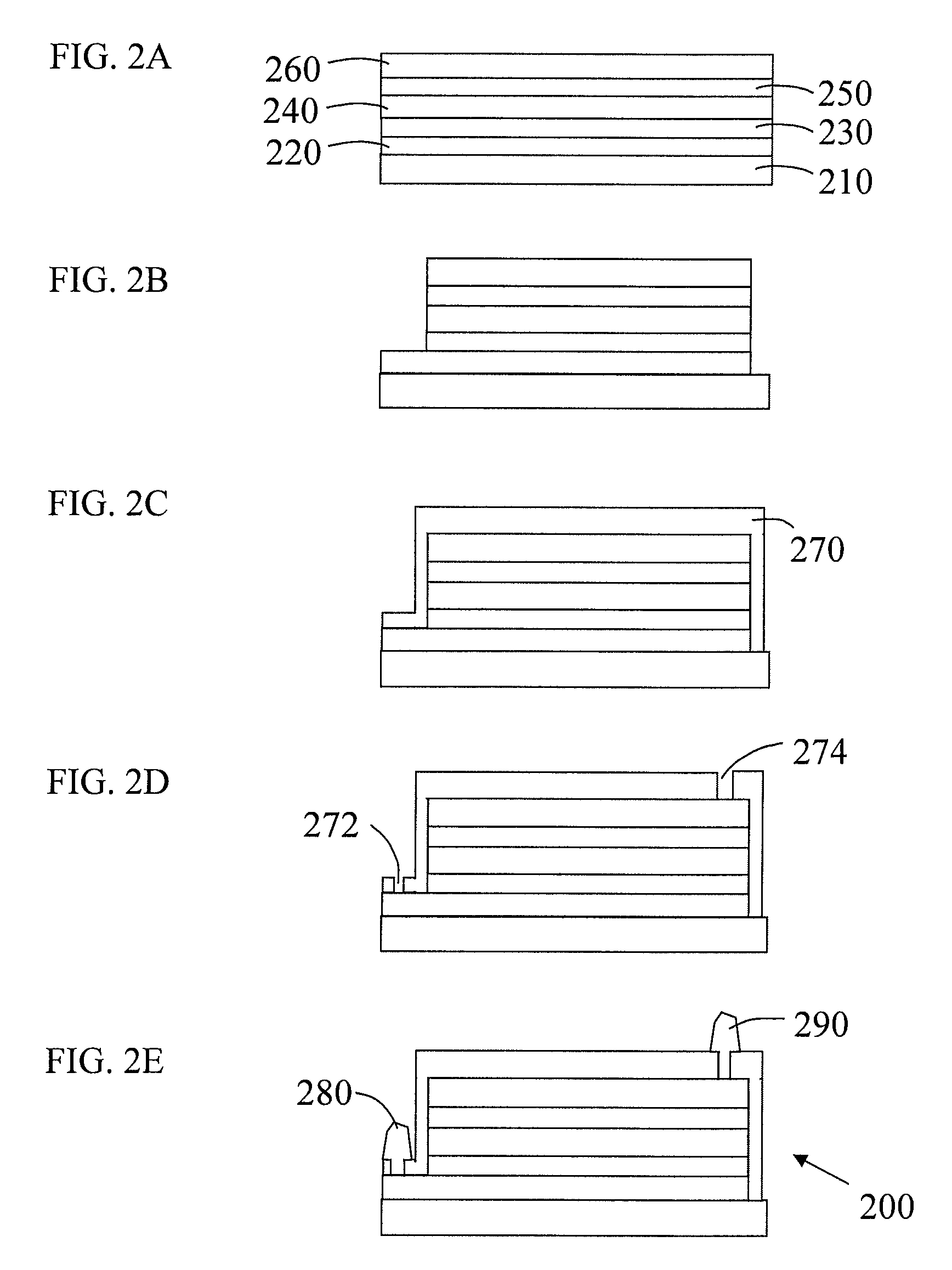
[0023]FIGS. 2A to 2E show a method for manufacturing an electrochromic device 200 according to the invention. FIG. 2A shows a stack of five layers which have been deposited on the substrate 210. The substrate may be glass or plastic. The layers, in order from the substrate, are lower transparent conductive oxide (TCO) layer 220, a cathode 230, a solid electrolyte 240, a counter electrode 250, and an upper TCO layer 260. The layers are deposited one after another using deposition techniques known to those skilled in the art. The lower and upper TCO layers 220 and 260 are typical sputter-deposited indium tin oxide (ITO). The cathode 230 and counter electrode are typically made of transition metal oxides and are typically deposited by physical vapor deposition methods. The solid electrolyte 240 is typically made of ceramic / oxide solid electrolytes such as lithium phosphorus oxynitride and LixSiO2, that can be deposited using various methods including physical and chemical vapor deposit...

second embodiment

[0024]In the method for manufacturing an electrochromic device according to the invention, the method according to FIGS. 2A through 2C is followed, then the electrical contacts are made through the barrier layer 270, without the need to open up contact areas 272 and 274 in the barrier layer 270. This method of making contact works by diffusing the contact material through the diffusion barrier layer to make an electrically conductive path. This results in the same final device as shown in FIG. 2E, except the first and second electrical contacts 280 and 290 sit on the diffusion barrier layer 270 and make electrical contact to the lower and upper TCO layers 220 and 260, respectively, through the diffusion barrier layer 270 (made locally conductive by contact material diffused into the diffusion barrier layer). This method is applicable when the diffusion barrier layer is either very thin or relatively porous. This may be the case when the demands on the diffusion barrier layer are les...


PUM

PropertyMeasurementUnit
transparent conductiveaaaaaaaaaa
transparentaaaaaaaaaa
depositionaaaaaaaaaa

Abstract

This invention contemplates the use of laser patterning / scribing in electrochromic device manufacture, anywhere during the manufacturing process as deemed appropriate and necessary for electrochromic device manufacturability, yield and functionality, while integrating the laser scribing so as to ensure the active layers of the device are protected to ensure long term reliability. It is envisaged that the laser is used to pattern the component layers of electrochromic devices by directly removing (ablating) the material of the component layers. The invention includes a manufacturing method for an electrochromic device comprising one or more focused laser patterning steps. To minimize redeposition of laser ablated material and particulate formation on device surfaces a number of approaches may be used: (1) ablated material generated by the focused laser patterning may be removed by vacuum suction and / or application of an inert gas jet in the vicinity of the laser ablation of device material; (2) spatial separation of the edges of layers and patterning of lower layers prior to deposition of upper layers; and (3) the laser patterning step may be performed by a laser beam focused directly on the deposited layers from above, by a laser beam directed through the transparent substrate, or by a combination of both.

Description

FIELD OF THE INVENTION[0001]The present invention relates generally to electrochromic devices, and more particularly to a method for fabricating electrochromic devices including laser patterning / scribing.BACKGROUND OF THE INVENTION[0002]Electrochromic devices are devices that change light (and heat) transmission properties in response to voltage applied across the device. Electrochromic devices can be fabricated which electrically switch between transparent and translucent states (where the transmitted light is colored). Furthermore, certain transition metal hydride electrochromic devices can be fabricated which switch between transparent and reflective states. Electrochromic devices are incorporated in a range of products, including architectural windows, rear-view mirrors, and protective glass for museum display cases. When they are incorporated in architectural windows there is a need for the electrochromic devices to have a guaranteed lifetime of at least ten years and preferabl...

Claims


Application Information

Patent Timeline
Patent Type & Authority Patents(United States)
IPC IPC(8): C08J7/18B05D3/06G02F1/15B05D5/06B05D5/12
CPCG02F1/1523G02F1/155G02F1/1533G02F2001/1536
Inventor KWAK, BYUNG SUNGKRISHNA, NETY
Owner APPLIED MATERIALS INC
Why Eureka
Try Eureka