Gate-all-around nanowire tunnel field effect transistors

a technology of field effect transistors and nanowire tunnels, which is applied in the field of gate-all-around nanowire tunnel field effect transistors, can solve the problems of undesirable junction doping profiles or unsatisfactory amorphization of nanowires

Active Publication Date: 2012-05-08
GLOBALFOUNDRIES US INC
View PDF79 Cites 36 Cited by
  • Summary
  • Abstract
  • Description
  • Claims
  • Application Information

AI Technical Summary

Problems solved by technology

Previous fabrication methods that used ion-implantation to dope the small diameter nanowire may result in undesirable amorphization of the nanowire or an undesirable junction doping profile.

Method used


Image

  • Gate-all-around nanowire tunnel field effect transistors
  • Gate-all-around nanowire tunnel field effect transistors
  • Gate-all-around nanowire tunnel field effect transistors

Examples


Embodiment Construction

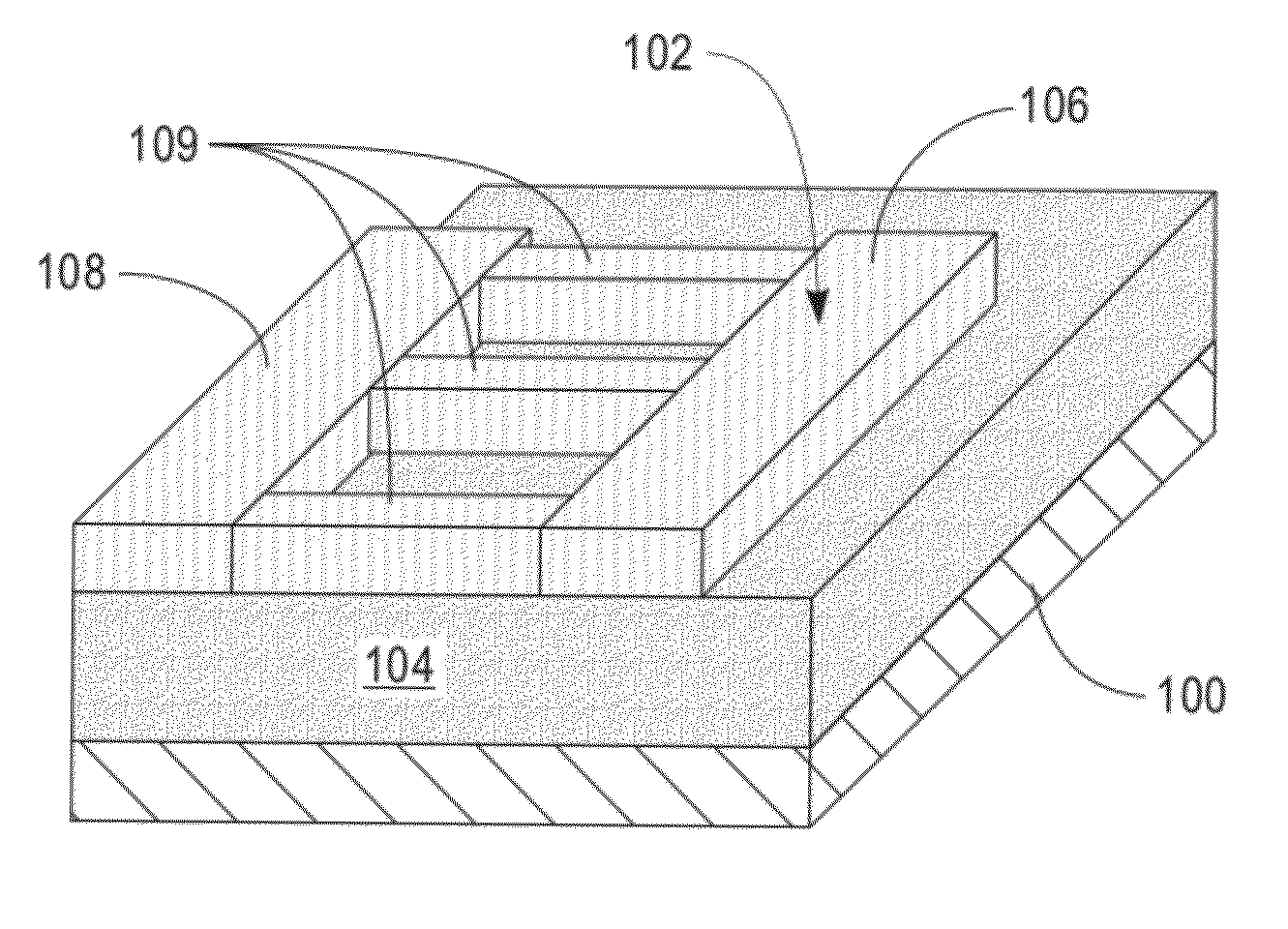
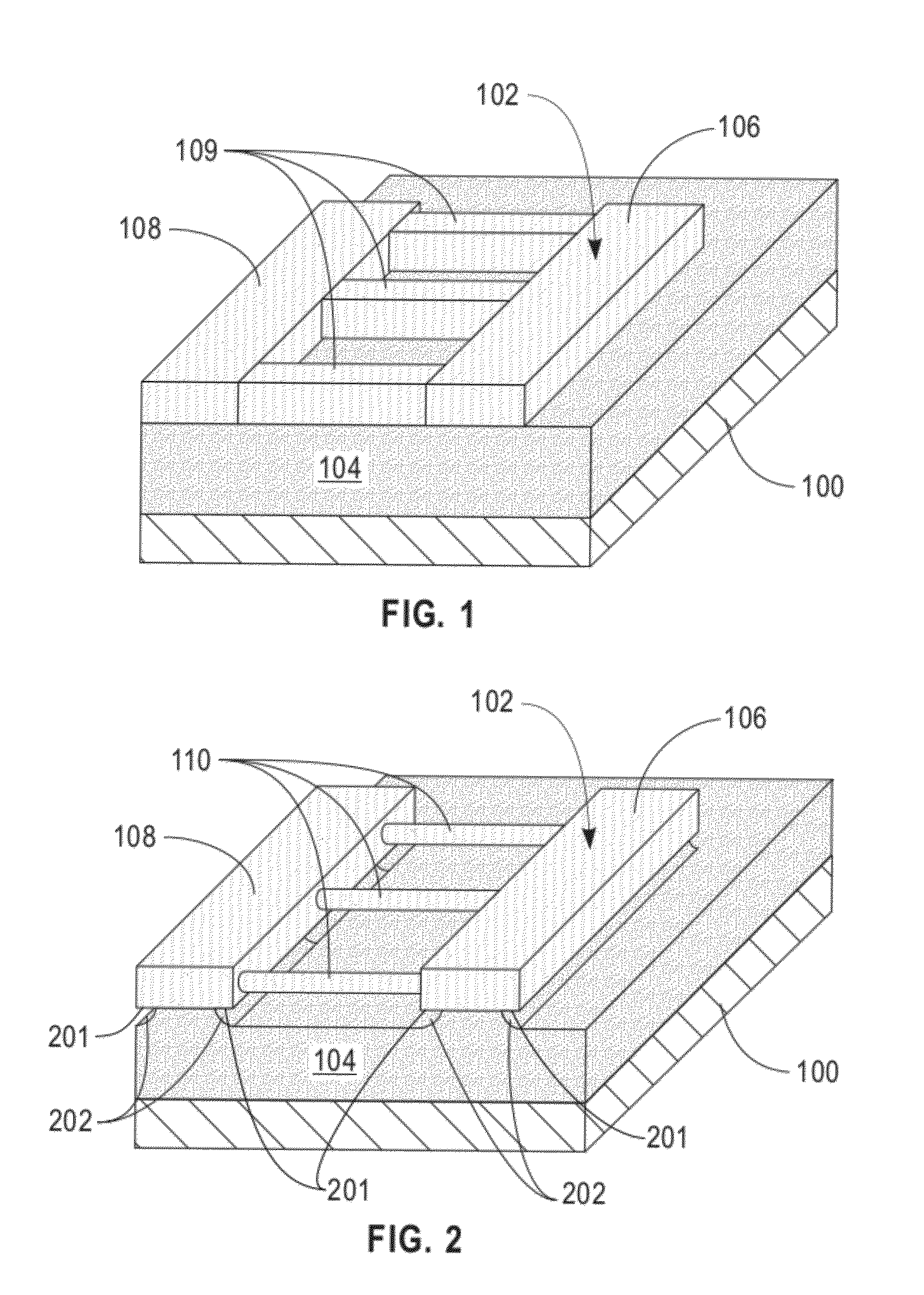
[0009]With reference now to FIG. 1, a silicon on insulator (SOI) portion 102 is defined on a buried oxide (BOX) layer 104 that is disposed on a silicon substrate 100. The SOI portion 102 includes a SOI pad region 106, a SOI pad region 108, and nanowire portions 109. The SOI portion 102 may be patterned by the use of lithography followed by an etching process such as, for example, reactive ion etching (RIE).

[0010]FIG. 2 illustrates the resultant BOX layer 104 and SOI portion 102 following an isotropic etching process. The BOX layer 104 is recessed in regions not covered by SOI portion 102. The isotropic etching results in the lateral etching of portions of the BOX layer 104 that are under the SOI portion 102. The lateral etch suspends the nanowires 109 above the BOX layer 104. The lateral etch forms the undercuts 202 in the BOX layer 104 and overhang portions 201 at the edges of SOI regions 106 and 108. The isotropic etching of the BOX layer 104 may be, for example, performed using a...


PUM


Abstract

A method for forming a nanowire tunnel field effect transistor (FET) device includes forming a nanowire suspended by first and second pad regions over a semiconductor substrate, the nanowire including a core portion and a dielectric layer, forming a gate structure around a portion of the dielectric layer, forming a first spacer around portions of the nanowire extending from the gate structure, implanting ions in a first portion of the nanowire, implanting ions in the dielectric layer of a second portion of the nanowire, removing the dielectric layer from the second portion of the nanowire, removing the core portion of the second portion of the exposed nanowire to form a cavity, and epitaxially growing a doped semiconductor material in the cavity from exposed cross sections of the nanowire and the second pad region to connect the exposed cross sections of the nanowire to the second pad region.

Description

CROSS REFERENCE TO RELATED APPLICATIONS[0001]This application is related to co-pending application Ser. No. 12 / 631,199, Ser. No. 12 / 631,205, Ser. No. 12 / 630,939, Ser. No. 12 / 631,213, Ser. No. 12 / 631,342, all of which are incorporated by reference herein.FIELD OF INVENTION[0002]The present invention relates to semiconductor nanowire tunnel field effect transistors.DESCRIPTION OF RELATED ART[0003]A nanowire tunnel field effect transistor (FET) includes doped portions of nanowire that contact the channel region and serve as source and drain regions of the device. Previous fabrication methods that used ion-implantation to dope the small diameter nanowire may result in undesirable amorphization of the nanowire or an undesirable junction doping profile.BRIEF SUMMARY[0004]In one aspect of the present invention, a method for forming a nanowire tunnel field effect transistor (FET) device includes forming a nanowire suspended by a first pad region and a second pad region over a semiconductor ...

Claims


Application Information

Patent Timeline
Patent Type & Authority Patents(United States)
IPC IPC(8): H01L29/12
CPCB82Y10/00B82Y40/00H01L29/0665H01L29/0673H01L29/42392H01L29/66439H01L29/775H01L29/78696H01L29/66469
Inventor BANGSARUNTIP, SARUNYACHANG, JOSEPHINE B.LAUER, ISAACSLEIGHT, JEFFREY W.
Owner GLOBALFOUNDRIES US INC
Why Eureka
Try Eureka