Semiconductor device and method of manufacturing the semiconductor device

a semiconductor and semiconductor technology, applied in the field of semiconductor devices, can solve the problems of increasing the risk of electrical resistance of interconnection, affecting the sealing effect of the cavity, and the inability to ensure the airtightness of the cavity without difficulty, so as to reduce the electric resistance of the interconnection and ensure the airtightness of the cavity

Active Publication Date: 2012-06-05
MITSUBISHI ELECTRIC CORP
View PDF17 Cites 0 Cited by
  • Summary
  • Abstract
  • Description
  • Claims
  • Application Information

AI Technical Summary

Benefits of technology

[0006]The invention has been made in view of the above, and an object of the invention is to provide a semiconductor device and a method of manufacturing the semiconductor device that can achieve both the ensuring of the airtightness of the cavity and the reduction in electric resistance of the interconnection.
[0011]In the semiconductor device according to one aspect of the invention, since the second interconnection having the thickness larger than the first thickness is arranged, the electric resistance of the interconnection for electrical connection to the element can be smaller than that in the case where only the interconnection of the first thickness is arranged. Since the 11 interconnection having the thickness smaller than the second thickness is arranged between the member and the substrate, occurrence of the irregularities at the upper surface of the member can be suppressed as compared with the case where only the interconnection of the second thickness is arranged. Therefore, the member and the cap can be joined closely. Therefore, the airtightness of the cavity can be ensured and also the electric resistance of the interconnection can be reduced.
[0012]In the semiconductor device according to another aspect of the invention, since the filling portion fills the concave portion formed between the side surface of the groove and the interconnection, the irregularities at the surface formed of the upper surfaces of the interconnection and the filling portion can be small even when the interconnection has a large thickness. Therefore, the occurrence of the irregularities at the upper surface of the member formed on this surface can be suppressed so that the member and the cap can be joined closely. Therefore, the airtightness of the cavity can be ensured and also the electric resistance of the interconnection can be reduced.
[0013]In the semiconductor device according to still another aspect of the invention, since the pattern is made of the same material as the interconnection, the interconnection and the pattern can be patterned collectively and thus simultaneously. Therefore, the pattern having the portion located on the opposite sides of the pattern can reduce the irregularities caused by the interconnection, without being affected by overlapping deviation.
[0014]In the method of manufacturing the semiconductor device of the invention, since the isotropic etching is performed for removing the insulating film not covered with the first mask layer, the edge of the insulating film has a gently stepped form. Therefore, the irregularities at the surface formed of the upper surfaces of the insulating film and the interconnection become gentle so that the irregularities at the upper surface of the member formed of the insulating film and the interconnection become small. Accordingly, the member and the cap can be closely joined together so that the airtightness of the cavity can be ensured.

Problems solved by technology

When the irregularities at the upper surface of the joint frame are excessively large, it is difficult to join closely the joint frame and the cap together, which results in a problem that airtightness of the cavity cannot be ensured without difficulty.
In particular, when a large shift or deviation occurs between the interconnection and the oxide film overlapped together, the irregularities at the upper surface of the joint frame become large, which makes the above problem more serious.
Thus, the above conventional method suffers from a problem that it is difficult to achieve both the ensuring of airtightness of the cavity and the reduction in electric resistance of the interconnection.

Method used


Image

  • Semiconductor device and method of manufacturing the semiconductor device
  • Semiconductor device and method of manufacturing the semiconductor device
  • Semiconductor device and method of manufacturing the semiconductor device

Examples


first embodiment

[0054](First Embodiment)

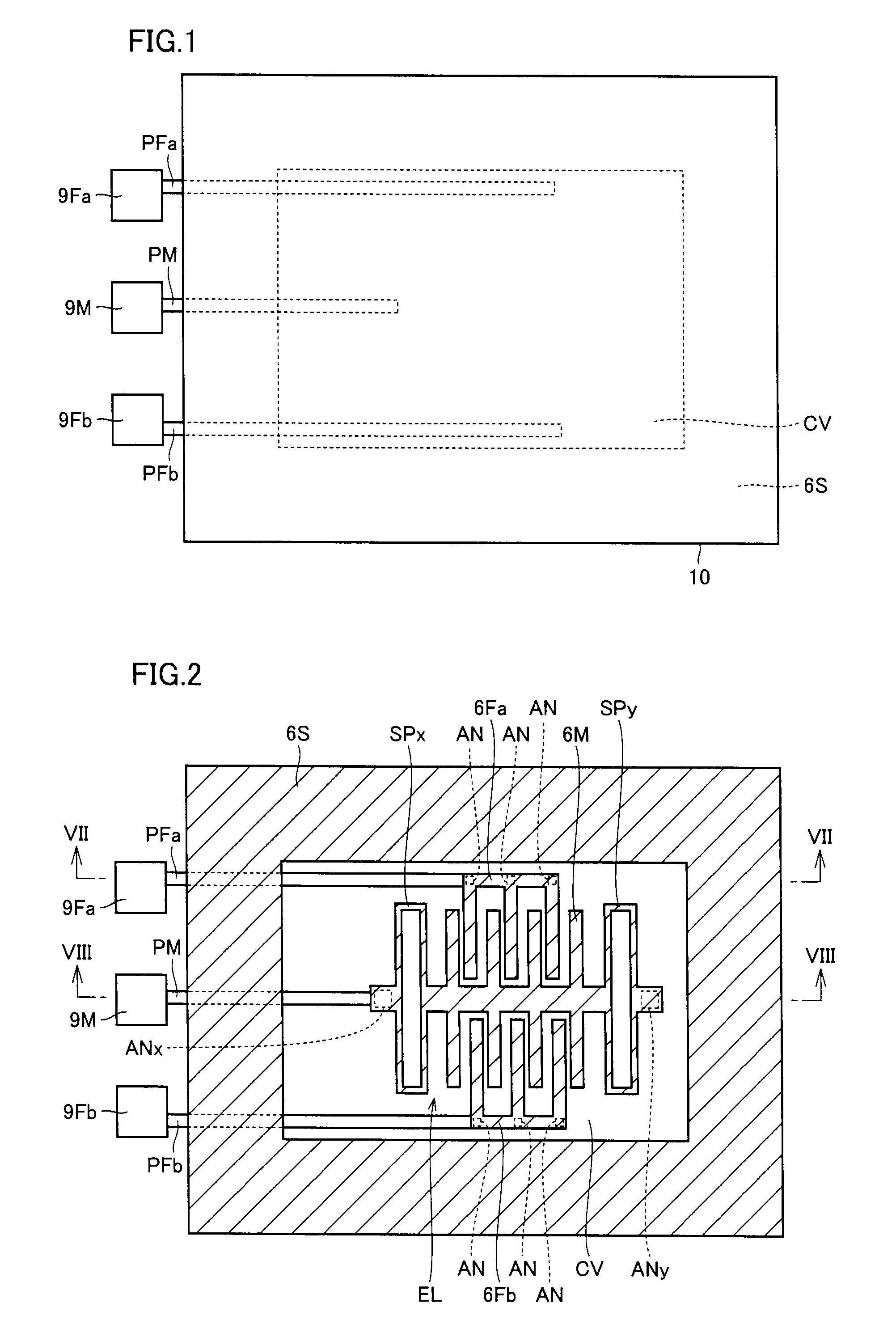
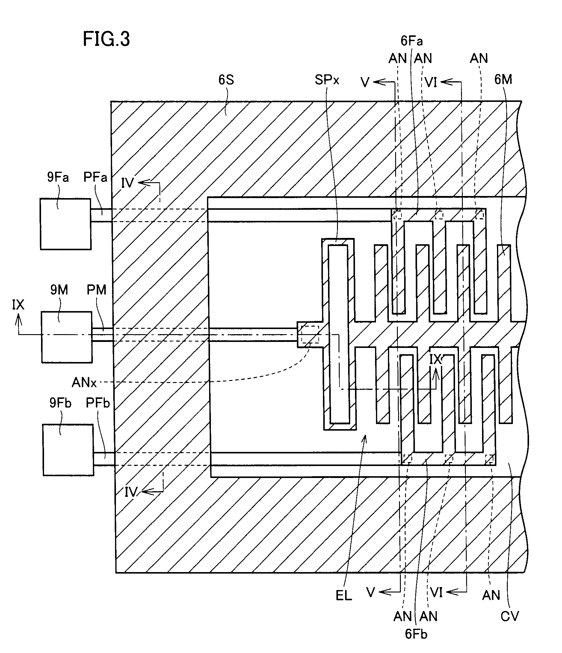
[0055]First, description will be given on a structure of an acceleration sensor that is a semiconductor device of a first embodiment.

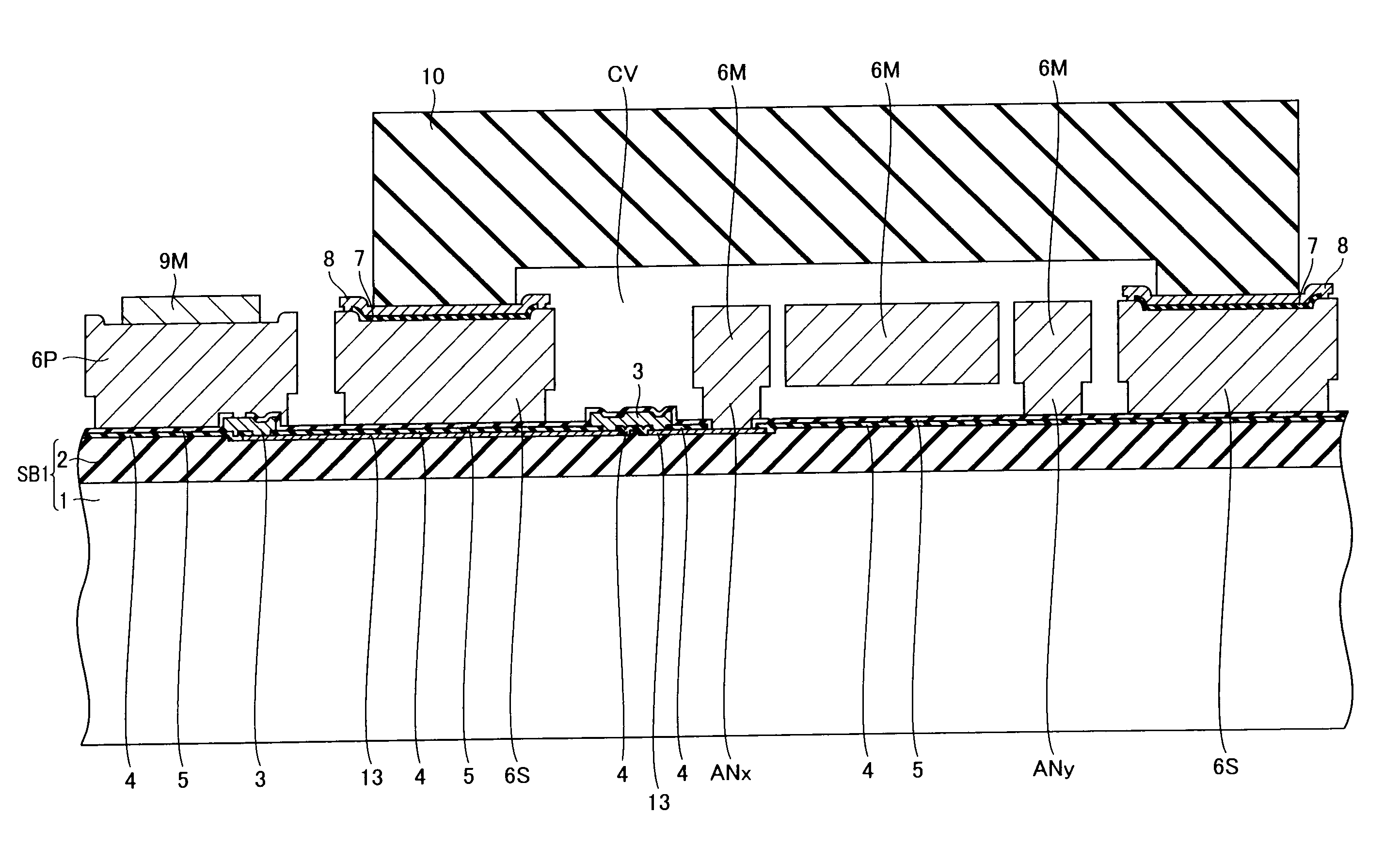
[0056]Referring primarily to FIG. 9, an acceleration sensor that is a semiconductor device of the first embodiment primarily has a substrate SB1, a doped polycrystalline silicon layer 13 (first interconnection), a doped polycrystalline silicon layer 3 (second interconnection), an acceleration sensing unit EL (element) in FIG. 2, a sealing unit 6S (member) and a cap 10.

[0057]Substrate SB1 has a silicon substrate 1 having a main surface, and an oxide film 2 formed on the main surface. Oxide film 2 has a groove formed on the side opposite to silicon substrate 1. Thus, substrate SB1 has the groove.

[0058]Doped polycrystalline silicon layer 13 extends along this groove and is located on the bottom surface thereof Doped polycrystalline silicon layer 13 is made of Doped Polycrystalline Silicon (DOPS). Impurities used for the doping are,...

second embodiment

[0094](Second Embodiment)

[0095]First, description will be given on a structure of an acceleration sensor that is a semiconductor device of a second embodiment.

[0096]Referring to FIGS. 28 and 29, the acceleration sensor of this embodiment includes a substrate SB2 having a groove instead of substrate SB1 (FIGS. 4 and 9) having the groove in the first embodiment. Substrate SB2 has silicon substrate 1 (the substrate member forming a bottom of the groove), an oxide film 2f and an oxide film 16 (the insulating film forming a side surface of the groove). Oxide film 2f is arranged on silicon substrate 1. For reducing a parasitic capacitance related to silicon substrate 1, oxide film 2f usually has a thickness of 1 μm or more. Oxide film 16 is formed selectively on oxide film 2f, and a region on oxide film 2f where oxide film 16 is not arranged forms the groove of substrate SB2.

[0097]Structures other than the above are substantially the same as those in the first embodiment already described...

third embodiment

[0105](Third Embodiment)

[0106]First, description will be given on a structure of an acceleration sensor that is a semiconductor device of a third embodiment.

[0107]Referring primarily to FIGS. 35 and 36, the acceleration sensor that is the semiconductor device of this embodiment primarily has a substrate SB3, a doped polycrystalline silicon layer 30 and an oxide film 40.

[0108]Substrate SB3 has silicon substrate 1 having a main surface, and oxide film 2f formed on this main surface. Oxide film 40 is formed on a part of oxide film 2f. A structure formed of substrate SB3 and oxide film 40 has a groove formed in a region where oxide film 40 is not formed on oxide film 2f.

[0109]Doped polycrystalline silicon layer 30 extends along this groove and is located on the bottom surface of the groove. Doped polycrystalline silicon layer 30 is formed of doped polycrystalline silicon. Impurities used for doping are, e.g., phosphorus (P). Doped polycrystalline silicon layer 30 has a thickness equal ...


PUM


Abstract

A first interconnection is formed along a groove of a substrate and on a bottom surface of the groove, and has a first thickness. A second interconnection is electrically connected to the first interconnection and has a second thickness larger than the first thickness. An acceleration sensing unit is electrically connected to the second interconnection. A sealing unit has a portion opposed to the substrate with the first interconnection therebetween, and surrounds the second interconnection and the acceleration sensing unit on the substrate. A cap is arranged on the sealing unit to form a cavity on a region of the substrate surrounded by the sealing unit. Thereby, airtightness of the cavity can be ensured and also an electric resistance of the interconnection connected to the acceleration sensing unit can be reduced.

Description

BACKGROUND OF THE INVENTION[0001]1. Field of the Invention[0002]The invention relates to a semiconductor device, and particularly to a semiconductor device provided with a cavity.[0003]2. Description of the Background Art[0004]A certain kind of semiconductor device has an element formed in a cavity. Particularly, when an element having a movable portion is arranged in a sealed cavity, characteristics of the element are improved in some cases. For example, according to Japanese Patent Laying-Open No. 2007-085747, a capacitance type acceleration sensor that is a semiconductor device has an acceleration sensing unit inside a cap (cavity) having airtightness. This cavity is defined by a substrate, a joint frame formed on the substrate and the cap joined to the joint frame. An interconnection held between oxide films extends through the joint frame.[0005]In a process of manufacturing the acceleration sensor, the joint frame is formed on a surface on which the interconnection is present. ...

Claims


Application Information

Patent Timeline
Patent Type & Authority Patents(United States)
IPC IPC(8): H01L23/48
CPCB81B7/007G01P15/0802G01P15/125G01P1/023B81B2207/097G01P2015/0814
Inventor SATO, KIMITOSHIOKUMURA, MIKAYAMAGUCHI, YASUOHORIKAWA, MAKIO
Owner MITSUBISHI ELECTRIC CORP
Why Eureka
Try Eureka