Hybrid time and frequency solution for PLL sub-block simulation

a phase lock loop and sub-block technology, applied in the field of semiconductor chip simulation, can solve the problems of too complicated phase lock loops, failure of integrated circuits, and problem of timing jitters of plls, and achieve the effect of avoiding the need for a separate simulation and a single simulation method

Active Publication Date: 2012-06-26
SYNOPSYS INC
View PDF5 Cites 1 Cited by
  • Summary
  • Abstract
  • Description
  • Claims
  • Application Information

AI Technical Summary

Problems solved by technology

However, with increasing frequency as well as larger process variation (from advanced manufacturing techniques), the timing jitters of PLLs have become problematic.
Specifically, the timing jitters may cause failure of an integrated circuit for various timing issues.
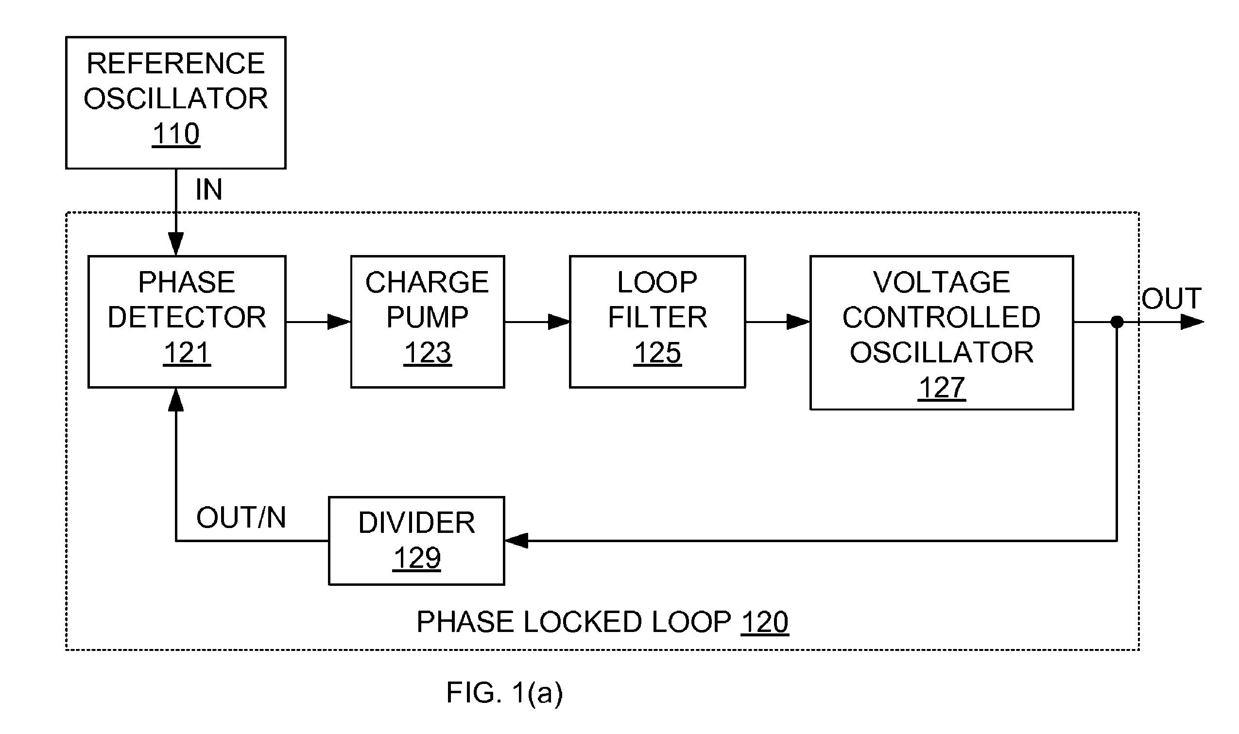
Phase lock loops are too complicated to be simulated directly.
However, the method of calculating timing jitter described above fails when the phase noise simulation of any sub-block fails.
Many sub-blocks of the PLL are very difficult to simulate.
In general “digital circuits” having input / output waveforms with sharp transitions and / or sharp corners are difficult to simulate.
Thus, phase detectors, frequency dividers (with high divide-by ratios) as well as voltage controlled oscillators in combination with frequency dividers are the most difficult to simulate.
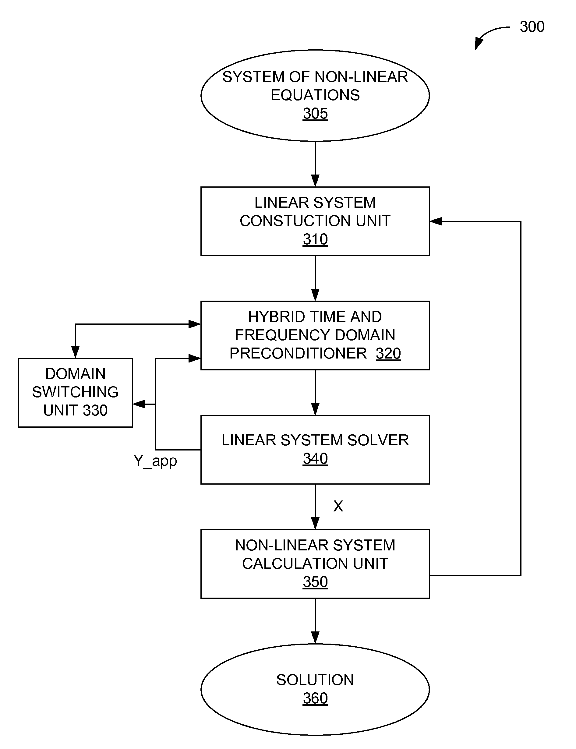
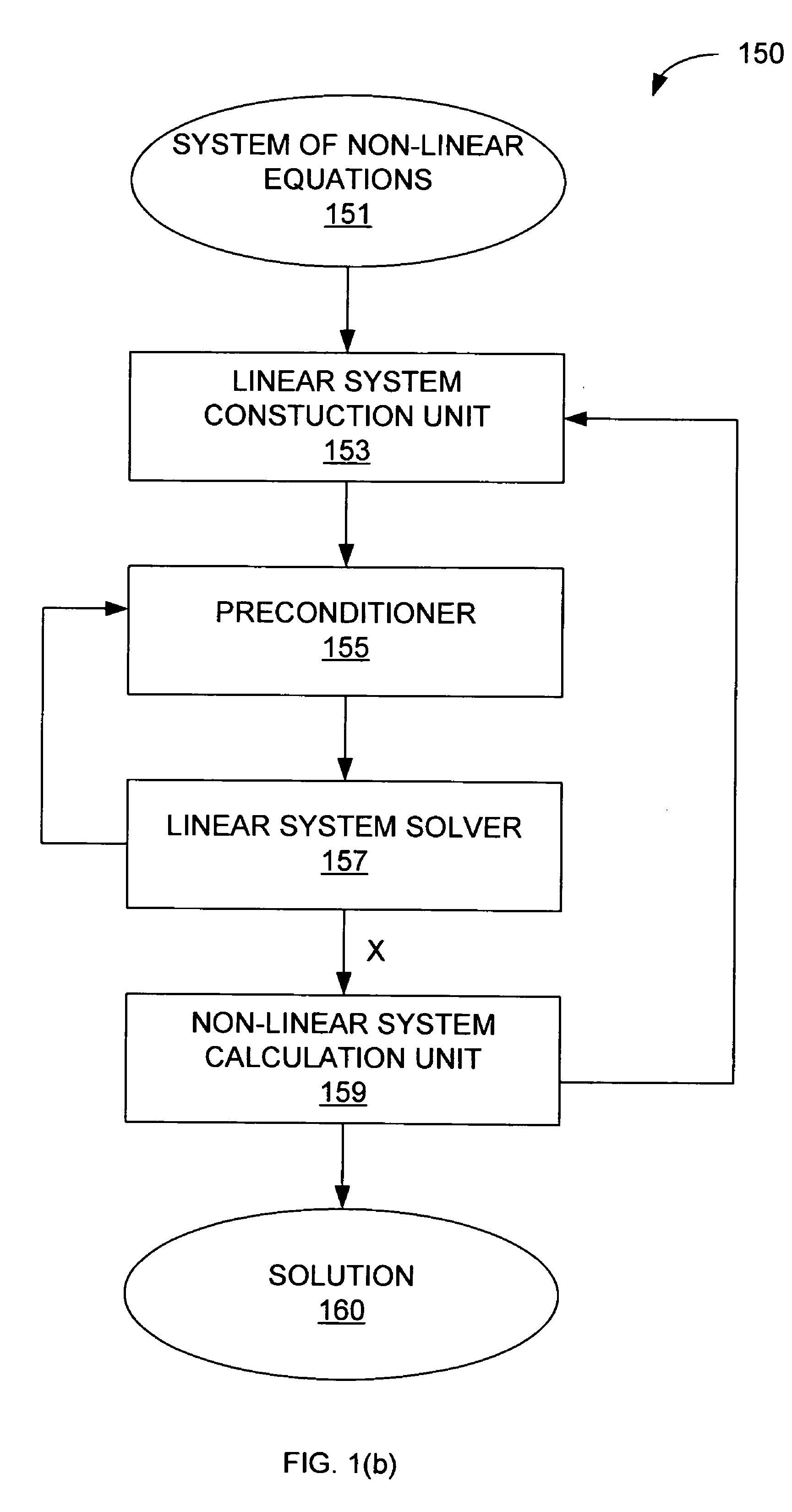
However, linear system solver 157 may not be able to solve or would take too long to solve most of system of linear equations generated by Newton's method.
However, even with preconditioner 155, linear system solver 157 might still not be able to solve the system of linear equations in a reasonable amount of time.
As explained above, the digital sub-blocks of phase lock loops are extremely difficult to simulate.
The difficulty results in very slow convergence or even divergence in linear system solver 157 even with the assistance of preconditioner 155.

Method used


Image

  • Hybrid time and frequency solution for PLL sub-block simulation
  • Hybrid time and frequency solution for PLL sub-block simulation
  • Hybrid time and frequency solution for PLL sub-block simulation

Examples


Embodiment Construction

[0023]It may be helpful to place the processes of this invention in context of the overall chip design. FIG. 2 shows a simplified representation of an exemplary digital IC design flow. At a high level, the process starts with the product idea (200) and is realized in a EDA software design process (210). When the design is finalized, it can be taped-out (event 240). After tape out, the fabrication process (250) and packaging and assembly processes (260) occur resulting, ultimately, in finished chips (result 270).

[0024]The EDA software design process (210) is actually composed of a number of stages 212-230, shown in linear fashion for simplicity. In an actual IC design process, the particular design might have to go back through steps until certain tests are passed. Similarly, in any actual design process, these steps may occur in different orders and combinations. This description is therefore provided by way of context and general explanation rather than as a specific, or recommende...


PUM


Abstract

A system for a fast method to simulate phase lock loop (PLL) sub-block simulation is presented. The simulation of the sub-blocks of the PLL involve solving a system of non-linear equations for the voltages and currents in the sub-blocks of the PLL. A harmonic balance method is used to solve the system of non-linear equation. The harmonic balance method involves creating a system of linear equations which is solved using a novel hybrid time and frequency domain preconditioner. The hybrid time and frequency domain preconditioner includes the strong and fast convergence property of time-domain preconditioning while avoiding the potential divergent problems of time-domain preconditioning. In addition the hybrid time and frequency domain preconditioner also includes the dependable convergence of frequency domain preconditioning while avoiding the potential stalling problems of frequency domain preconditioning.

Description

BACKGROUND[0001]1. Field of the Invention[0002]The invention relates to simulation of semiconductor chips. More specifically, the invention relates to a method and an apparatus for simulating phase lock loops (PLLs) in integrated circuits.[0003]2. Related Art[0004]Most integrated circuits include one or more phase locked loops (PLL) for clock synthesis, clock and data recovery circuits, or frequency synthesis circuits. When integrated circuits ran at relatively low frequencies (clock speeds), timing jitters within the PLLs were not significant and were generally ignored. However, with increasing frequency as well as larger process variation (from advanced manufacturing techniques), the timing jitters of PLLs have become problematic. Specifically, the timing jitters may cause failure of an integrated circuit for various timing issues. Thus, to properly simulate an integrated circuit the timing jitters of any phase locked loops within the integrated circuit must also be accurately sim...

Claims


Application Information

Patent Timeline
Patent Type & Authority Patents(United States)
IPC IPC(8): G06F7/60G06F17/10
CPCG06F17/5036G06F30/367
Inventor BOUARICHA, ALI
Owner SYNOPSYS INC
Why Eureka
Try Eureka