Metal wiring layer and method of fabricating the same

a metal wiring and metal technology, applied in the direction of electrical equipment, semiconductor devices, semiconductor/solid-state device details, etc., can solve the problems of liquid crystal layer deterioration, liquid crystal layer may not be properly filled with liquid crystal molecules, and the step difference between a substrate and the metal wiring may increase, so as to prevent the occurrence of a build-up phenomenon and reduce the step difference

Active Publication Date: 2012-07-03
SAMSUNG DISPLAY CO LTD
View PDF12 Cites 7 Cited by
  • Summary
  • Abstract
  • Description
  • Claims
  • Application Information

AI Technical Summary

Benefits of technology

[0009]One or more embodiments of the present invention provide a metal wiring layer and a method of forming the same capable of preventing the occurrence of a build-up phenomenon during the formation of a buried-type metal wiring layer in a trench on a substrate, and thus capable of reducing a step difference.
[0010]One or more embodiments of the present invention also provide a metal wiring layer and a method of forming the same capable of preventing the occurrence of an edge build-up phenomenon in a buried-type metal wiring layer by forming a dielectric layer on a substrate, patterning the dielectric layer through etching so as to have a hole in the dielectric layer having a cross sectional area decreasing with increasing distance away from the substrate, and then forming a trench in the substrate through etching.
[0021]In accordance with another embodiment of the present invention, a cross sectional area of the trench may decrease with increasing distance into the substrate.

Problems solved by technology

However, as the width of metal wiring increases, the area of pixel regions decreases, and thus, the transmittance of a liquid crystal layer deteriorates.
Furthermore, as the thickness of metal wiring increases, a step difference between a substrate and the metal wiring may increase.
When a lower substrate has such a huge step difference, a liquid crystal layer may not be properly filled with liquid crystal molecules.
As a result, the transmittance of the liquid crystal layer may become irregular due to an irregular alignment of liquid crystal molecules in the liquid crystal layer, and the quality of display may deteriorate.
These methods, however, may result in various defects such as an edge build-up phenomenon, in which a metal layer is excessively grown along the edges of a trench and thus the metal layer becomes thicker near the edges than at other regions in the trench.

Method used


Image

  • Metal wiring layer and method of fabricating the same
  • Metal wiring layer and method of fabricating the same
  • Metal wiring layer and method of fabricating the same

Examples


Embodiment Construction

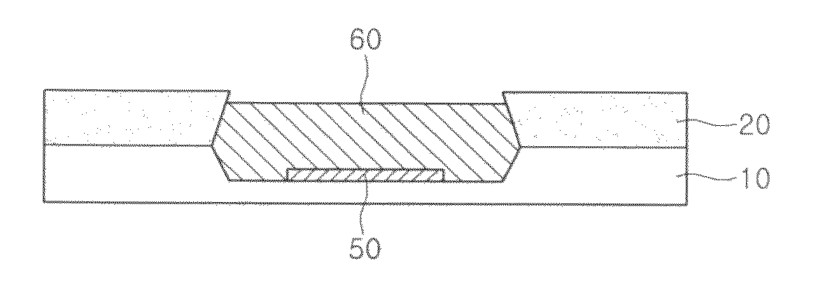
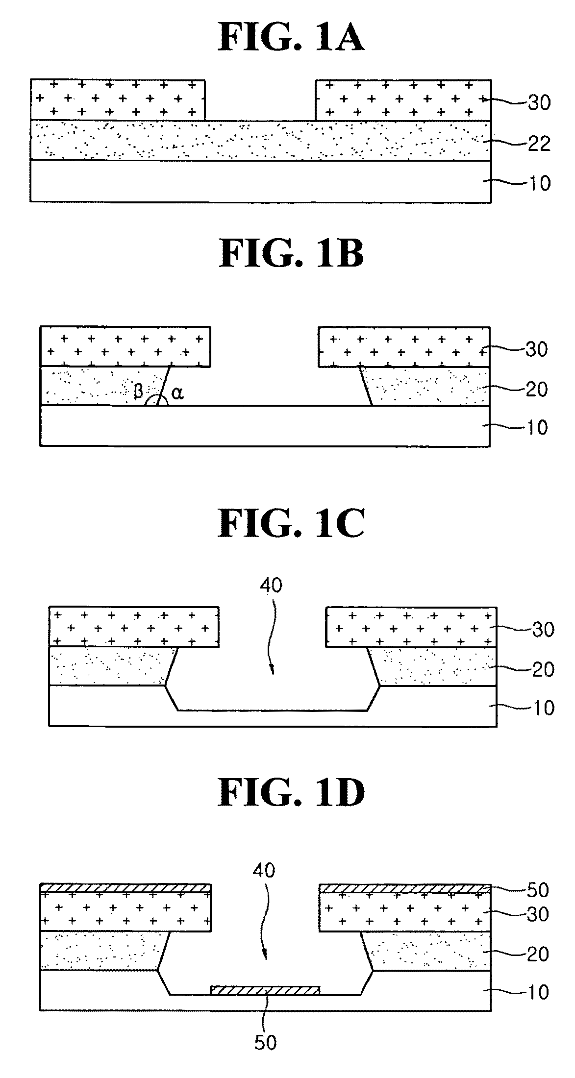
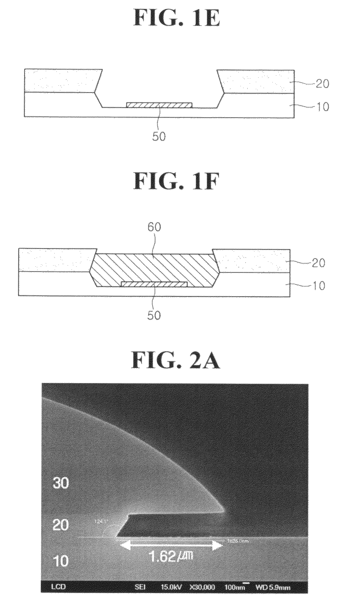
[0048]Embodiments of the present invention will now be described more fully with reference to the accompanying drawings, in which one or more exemplary embodiments of the invention are shown. The invention may, however, be embodied in many different forms and should not be construed as being limited to the embodiments set forth herein. Rather, these embodiments are provided so that this disclosure will be thorough and complete, and will fully convey the concept of the invention to those skilled in the art.

[0049]It will be understood that when an element is referred to as being “connected” or “coupled” to another element, it may be directly connected or coupled to the other element, or intervening elements may be present. In contrast, when an element is referred to as being “directly connected” or “directly coupled” to another element, there are no intervening elements present. Like reference numerals refer to like elements throughout. As used herein, the term “and / or” includes any a...


PUM

PropertyMeasurementUnit
internal angleaaaaaaaaaa

Abstract

A metal wiring layer and a method of fabricating the metal wiring layer are provided. The method includes forming a dielectric layer on a substrate, forming a plurality of dielectric layer patterns and holes therein on the substrate by etching part of the dielectric layer, with a cross sectional area of the holes in the dielectric layer patterns decreasing with increasing distance away from the substrate and the holes exposing the substrate, forming a trench by etching a portion of the substrate exposed through the holes in the dielectric layer patterns, and forming a metal layer which fills the trench and the holes in the dielectric layer patterns. Thus, it is possible to prevent the occurrence of an edge build-up phenomenon by forming a metal layer in a plurality of holes in the dielectric layer patterns having a cross sectional area decreasing with increasing distance away from the substrate. Therefore, it is possible to prevent the transmittance of a liquid crystal layer from decreasing due to a failure to properly fill liquid crystal molecules in the liquid crystal layer, and thus to increase the quality of display.

Description

CROSS-REFERENCE TO RELATED APPLICATION[0001]This application claims priority to and the benefit of Korean Patent Application No. 10-2007-0112342 filed on Nov. 5, 2007 in the Korean Intellectual Property Office, the disclosure of which is incorporated herein by reference in its entirety.BACKGROUND[0002]1. Technical Field[0003]One or more embodiments of the present invention generally relate to a metal wiring layer, and a method of fabricating the same. More particularly, one or more embodiments of the present invention relate to a buried-type metal wiring layer, and a method of fabricating the same.[0004]2. Description of the Related Art[0005]As a flat panel display, a liquid crystal display (LCD) includes a lower substrate on which a plurality of gate lines, a plurality of data lines, a plurality of pixel electrodes and a plurality of thin-film transistors (TFTs) are formed, an upper substrate on which a common electrode is formed, and a liquid crystal layer which is interposed betw...

Claims


Application Information

Patent Timeline
Patent Type & Authority Patents(United States)
IPC IPC(8): H01L21/44
CPCH01L21/743H01L23/535H01L27/1218H01L27/124H01L2924/0002H01L2924/00H01L21/28
Inventor YANG, DONG-JUCHOI, SHIN-ILKIM, SANG-GABOH, MIN-SEOKCHIN, HONG-KEELEE, KI-YEUPJEONG, YU-GWANGCHOI, SEUNG-HA
Owner SAMSUNG DISPLAY CO LTD
Why Eureka
Try Eureka