Photoelectric converter and photoelectric conversion element

a conversion element and photoelectric technology, applied in the direction of photometry using electric radiation detectors, instruments, radioation controlled devices, etc., can solve the problems of low sensitivity and low s/n ratio, and achieve high sensitivity and high s/n ratio

Active Publication Date: 2012-07-03
SONY CORP
View PDF10 Cites 9 Cited by
  • Summary
  • Abstract
  • Description
  • Claims
  • Application Information

AI Technical Summary

Benefits of technology

[0060]In the photoelectric conversion element and the like according to embodiments of the present invention, when a constant amount of light is applied to the photoelectric conversion material layer while a voltage is applied between the first electrode and the second electrode (that is, while a bias voltage is applied between the first electrode and the second electrode), a current generated in the photoelectric conversion material layer changes with the lapse of an application time. Consequently, a photoelectric conversion element and the like having high sensitivity and high S / N ratio can be provided by detecting the above-described change in the current. That is, the amount of received light can be determined on the basis of the discharge current, and the discharge current provides a large signal as compared with that of a steady-state current. Therefore, a photoelectric conversion element and the like can be provided while having advantages that the amount of received light can be calculated from a weak signal in low voltage drive (2 V or less) in which the S / N ratio decreases and the amount of light can be reliably calculated even when the amount of light is very small and the S / N ratio decreases because of the characteristics of the discharge current. When the light is applied to the photoelectric conversion material layer, regarding the current-time response and the dependence on the amount of light in the application of light, the current area (the integral of the current with respect to time) of the transient discharge current is dependent on the amount of light and, in addition, the time constant τ of the transient discharge current increases in the region of a small amount of light.

Problems solved by technology

However, reading of such steady-state parts of output signals have problems in that the sensitivity is low and the S / N ratio is low.

Method used


Image

  • Photoelectric converter and photoelectric conversion element
  • Photoelectric converter and photoelectric conversion element
  • Photoelectric converter and photoelectric conversion element

Examples


example 1

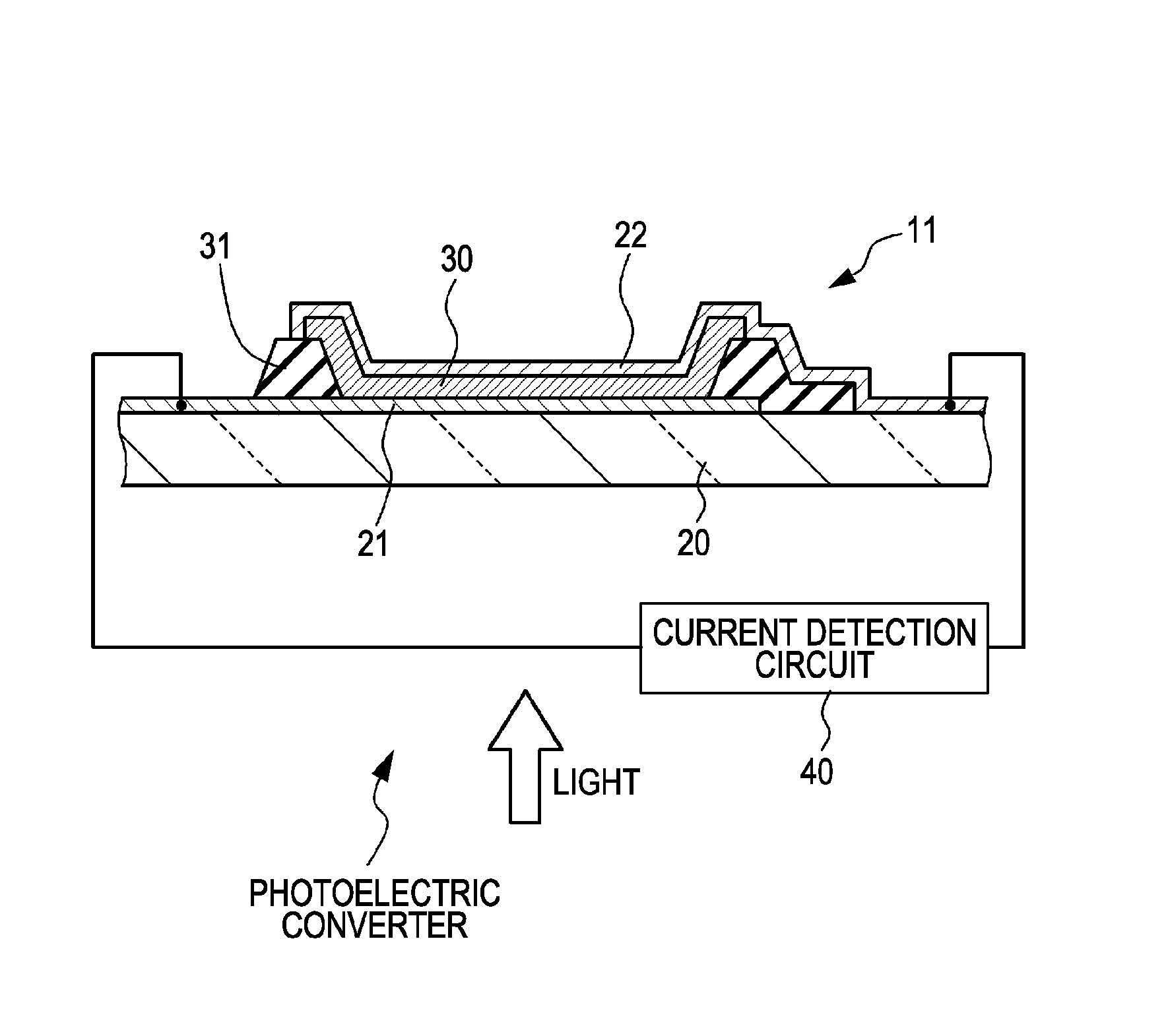
[0070]Example 1 relate to a photoelectric converter and a photoelectric conversion element according to embodiments of the present invention. In particular, the photoelectric conversion element in Example 1 is a first configuration photoelectric conversion element. As is indicated by a schematic sectional view shown in FIG. 1, a photoelectric conversion element 11 in Example 1 includes (A) a first electrode 21 and a second electrode 22 disposed discretely and (B) a photoelectric conversion material layer 30 disposed between the first electrode 21 and the second electrode 22. Furthermore, a photoelectric converter in Example 1 includes the photoelectric conversion element 11 and, in addition, includes a current detection circuit 40.

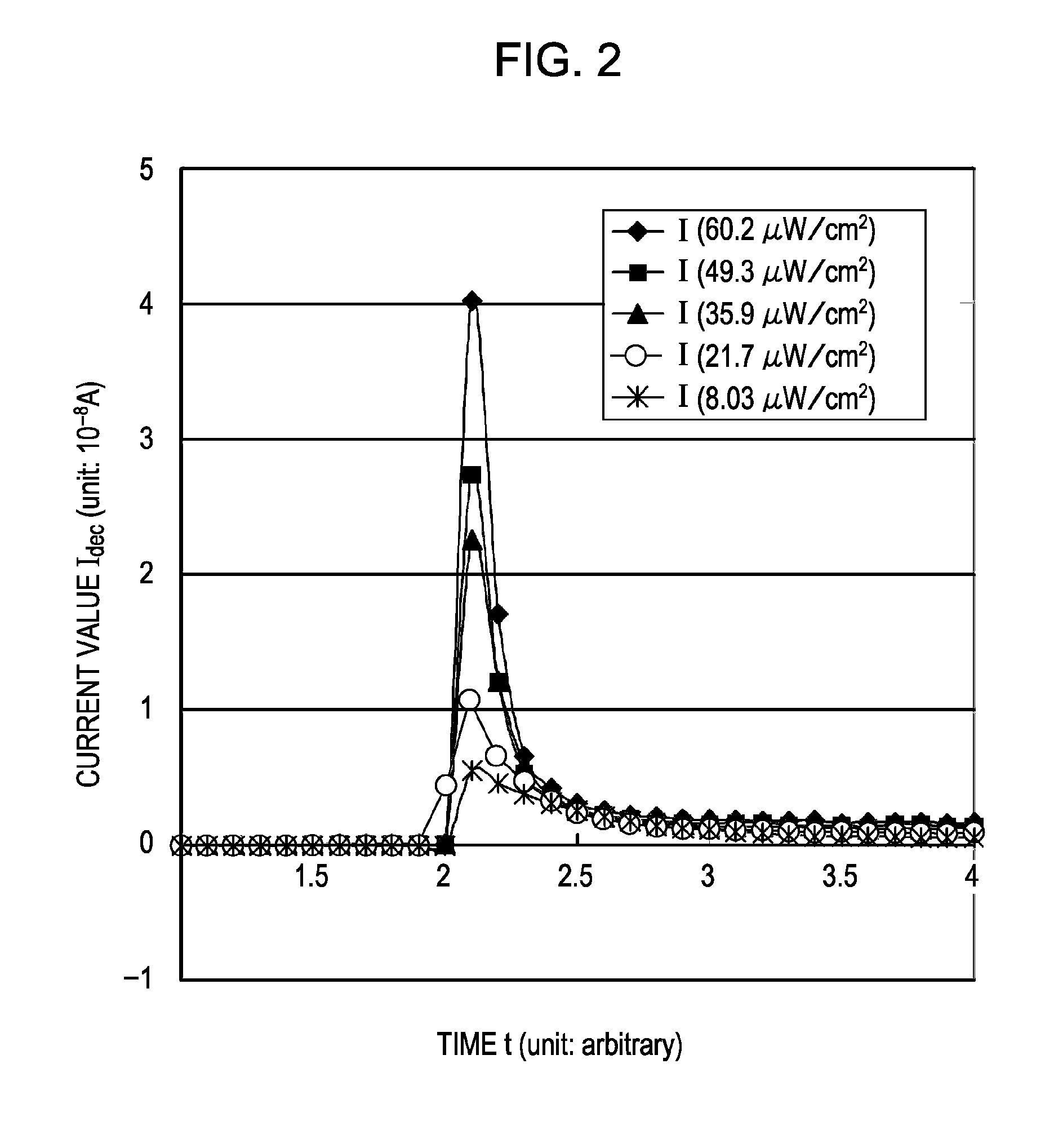
[0071]Then, in the photoelectric conversion element 11 in Example 1 or in the photoelectric conversion element 11 constituting the photoelectric converter in Example 1, when a constant amount of light is applied to the photoelectric conversion material lay...

example 2

[0081]Example 2 is a modification of Example 1. The photoelectric conversion element 12 in Example 2 is a second configuration photoelectric conversion element. That is, as is indicated by a schematic partial sectional view shown in FIG. 6A, a first electrode 21A is disposed on a substrate 20A, a photoelectric conversion material layer 30 is disposed on the first electrode 21A, and a second electrode 22A formed from a transparent material is disposed on the photoelectric conversion material layer 30. The light is incident on the photoelectric conversion material layer 30 through the second electrode 22A. Here, specifically, the substrate 20A is formed from, for example, a silicon semiconductor substrate, the first electrode 21A is formed from aluminum, and the second electrode 22A is formed from ITO. The configuration and the structure of the photoelectric conversion element 12 or a photoelectric converter in Example 2 may be the same configuration and structure as those of the phot...

example 3

[0082]Example 3 is also a modification of Example 1. The photoelectric conversion element 13 in Example 3 is a third configuration photoelectric conversion element. That is, as is indicated by a schematic partial sectional view shown in FIG. 6B, a first electrode 21B and a second electrode 22B are disposed on a substrate. A photoelectric conversion material layer 30 is disposed on the substrate 20B while extending from the first electrode 21B to the second electrode 22B. The light is incident on the photoelectric conversion material layer 30 through the second electrode 22B. Alternatively, the light is incident on the photoelectric conversion material layer 30 through the substrate 20B and the first electrode 21B. Here, specifically, the substrate 20B is formed from, for example, a silicon semiconductor substrate, the first electrode 21B and the second electrode 22B are formed from a metal material or a transparent electrically conductive material. The configuration and the structur...


PUM


Abstract

A photoelectric converter includes a photoelectric conversion element, which includes a first electrode and a second electrode disposed discretely and a photoelectric conversion material layer disposed between the first electrode and the second electrode and in which a current generated in the photoelectric conversion material layer changes with the lapse of an application time, where a constant amount of light is applied to the photoelectric conversion material layer while a voltage is applied between the first electrode and the second electrode, and a current detection circuit to detect the change in the current.

Description

BACKGROUND OF THE INVENTION[0001]1. Field of the Invention[0002]The present invention relates to a photoelectric conversion element and a photoelectric converter including the photoelectric conversion element.[0003]2. Description of the Related Art[0004]Photoelectric conversion elements, e.g., image sensors, usually have a structure in which a photoelectric conversion part is sandwiched between two electrodes. Then, an output (for example, current) from the photoelectric conversion element has no time dependence and is detected as a steady-state output (steady-state current). This is because a semiconductor material typified by silicon (Si) forms an electric double layer instantaneously and gives a steady-state current at commonly used electric field strength.[0005]For example, Japanese Unexamined Patent Application Publication No. 2006-100797 discloses an imaging element, in which a photoelectric conversion part is formed from an organic semiconductor material. This imaging element...

Claims


Application Information

Patent Timeline
Patent Type & Authority Patents(United States)
IPC IPC(8): G01J1/44
CPCH01L27/305H01L51/428Y02E10/549H10K39/30H10K30/65H01L27/146
Inventor MURATA, MASAKI
Owner SONY CORP
Why Eureka
Try Eureka