Semiconductor integrated circuit device and a method of manufacturing the same

a technology of integrated circuit devices and semiconductors, applied in semiconductor devices, diodes, electrical devices, etc., can solve problems such as abnormal heat generation, and achieve the effect of reducing the influence of another process parameter on device characteristics

Active Publication Date: 2012-07-17
RENESAS ELECTRONICS CORP
View PDF5 Cites 2 Cited by
  • Summary
  • Abstract
  • Description
  • Claims
  • Application Information

AI Technical Summary

Benefits of technology

[0011]Conventionally, a circuit for preventing the latch-up has been constructed with a Schottky barrier diode manufactured as a discrete product, and mounted as external circuitry in an LCD driver. According to the study conducted by the present inventors, the recent demand trend for LCDs shows a rapid increase in the number of LCDs mounted in mobile communication terminals and the like. For this or other reasons, LCD drivers have been required to be implemented as small-size chips, and reduced in power consumption so that a technology which embeds a Schottky barrier diode in an LCD driver has been devised. It has been particularly desired to implement a space-saving and low-power-consumption LCD driver at low cost by embedding a Schottky barrier diode in a chip forming the LCD driver.
[0019]That is, by collectively arranging the contact electrodes of a Schottky barrier diode of a type embedded in a semiconductor integrated circuit device over a guard ring in contact with a peripheral isolation region, it is possible to reduce the influence of another process parameter on device characteristics.

Problems solved by technology

In not only the LDC driver, but also a driving integrated circuit used in a portion close to a power source, a reverse current introduced into a main device by, e.g., voltage inversion at the time of application of a power source voltage may cause a so-called latch-up phenomenon which brings about abnormal heat generation particularly in a parasitic element or the like.

Method used


Image

  • Semiconductor integrated circuit device and a method of manufacturing the same
  • Semiconductor integrated circuit device and a method of manufacturing the same
  • Semiconductor integrated circuit device and a method of manufacturing the same

Examples


Embodiment Construction

Outline of Embodiments

[0107]First, a description will be given of the outline of the representative embodiments of the invention disclosed in the present application.

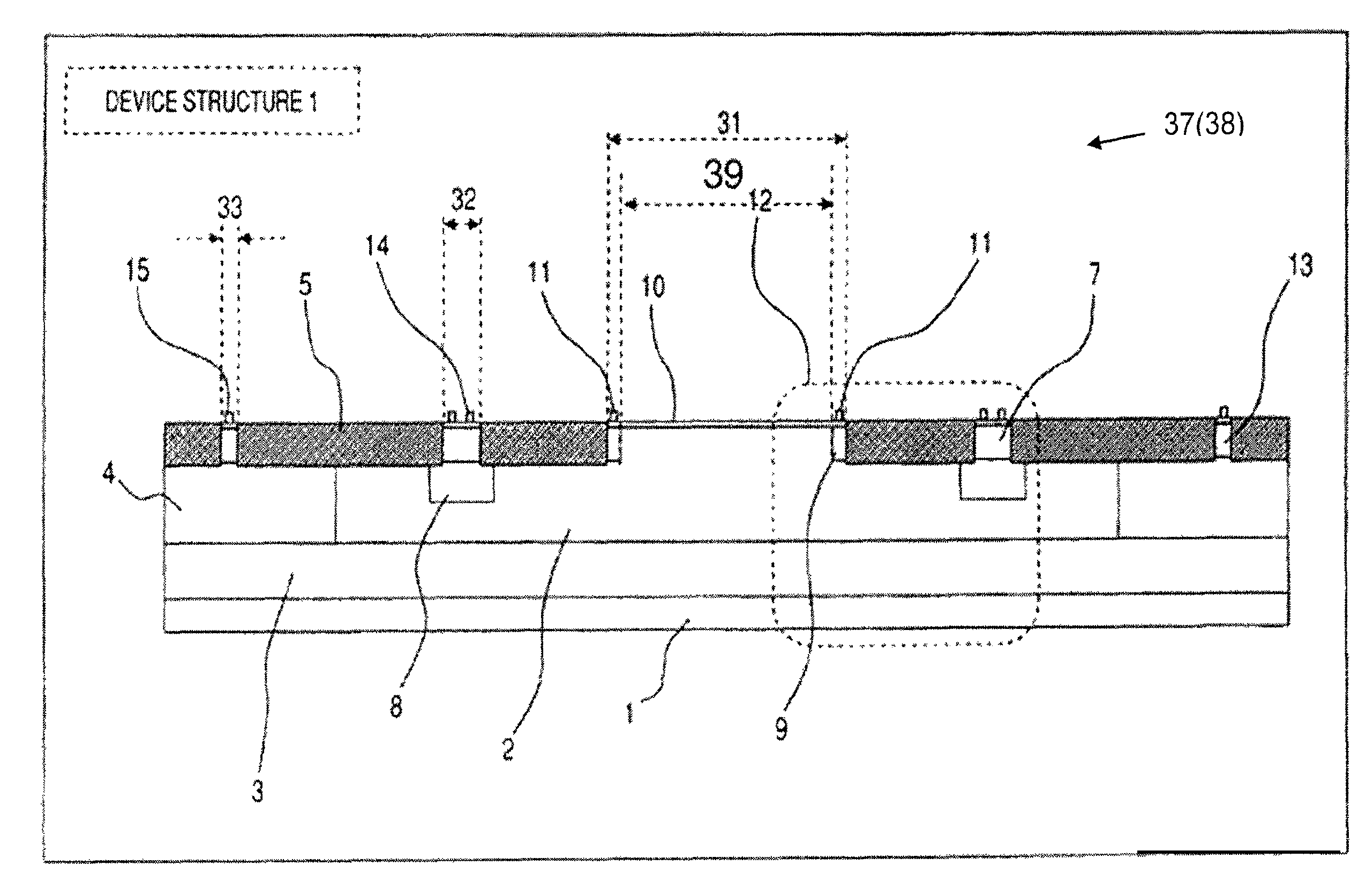
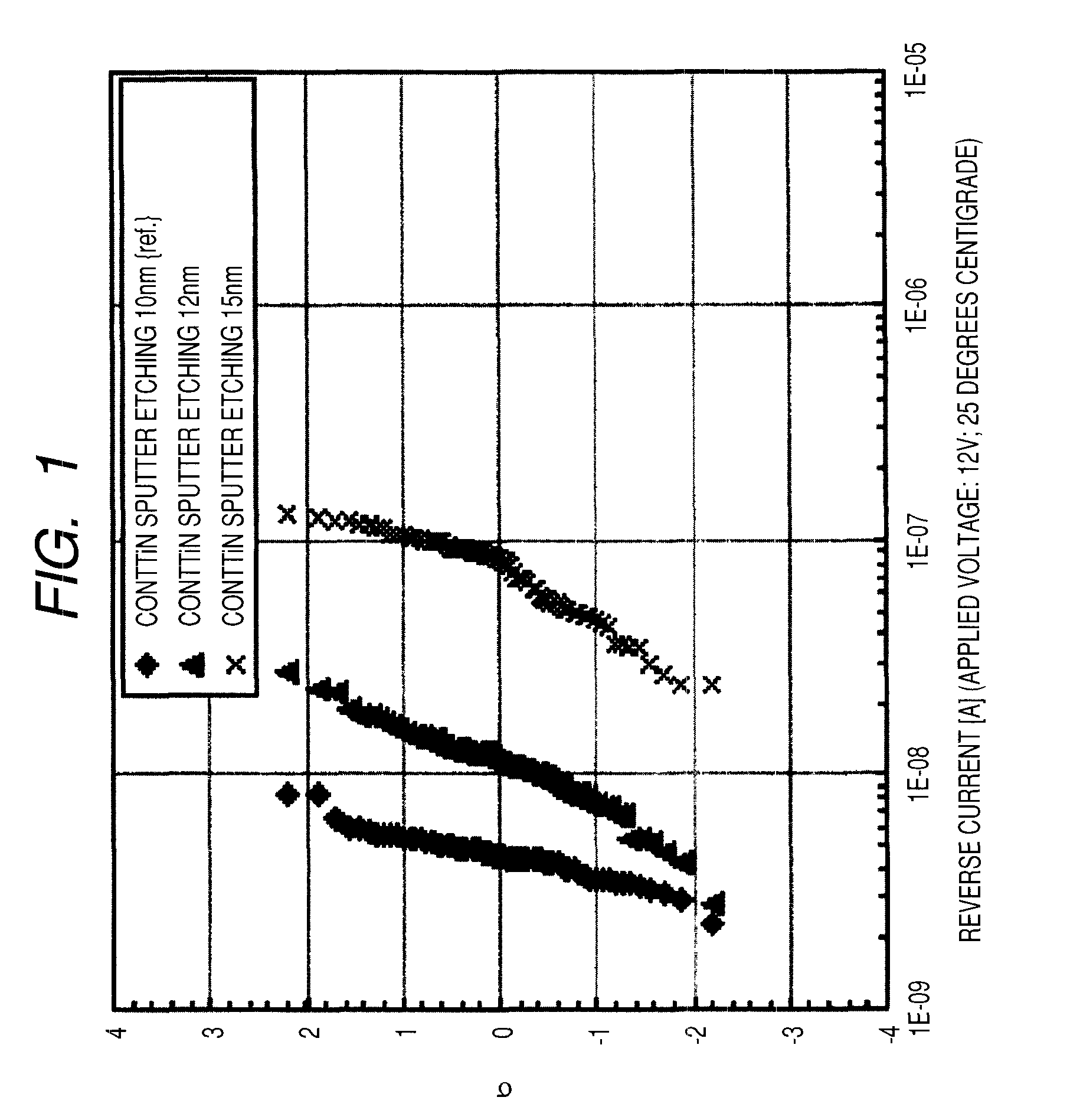
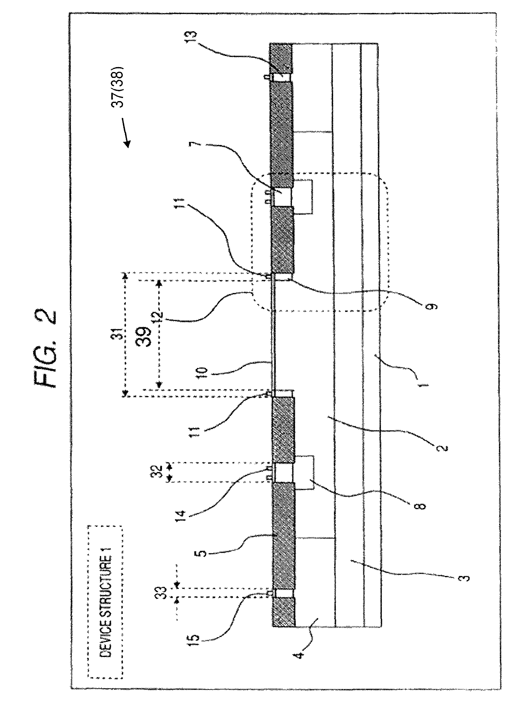
[0108]1. A semiconductor integrated circuit device includes: (a) a semiconductor substrate having a first principal surface and a second principal surface; (b) a CMOS integrated circuit portion provided in a first region of the first principal surface of the semiconductor substrate; and (c) a Schottky barrier diode portion provided in a second region of the first principal surface of the semiconductor substrate, wherein the Schottky barrier diode portion includes: (c1) a first N-type semiconductor region provided in the first principal surface in the second region; (c2) a first field insulating film region having an opening and provided in the first principal surface in the first N-type semiconductor region; (c3) a P-type guard ring region provided in the first principal surface in the opening of the first field insulat...


PUM


Abstract

To achieve a further reduction in the size of a finished product by reducing the number of externally embedded parts, the embedding of a Schottky barrier diode which is relatively large in the amount of current in a semiconductor integrated circuit device has been pursued. In such a case, it is general practice to densely arrange a large number of contact electrodes in a matrix over a Schottky junction region. It has been widely performed to perform a sputter etching process with respect to the surface of a silicide layer at the bottom of each contact hole before a barrier metal layer is deposited. However, in a structure in which electrodes are thus arranged over a Schottky junction region, a reverse leakage current in a Schottky barrier diode is varied by variations in the amount of sputter etching. The present invention is a semiconductor integrated circuit device having a Schottky barrier diode in which contact electrodes are arranged over a guard ring in contact with a peripheral isolation region.

Description

CROSS-REFERENCE TO RELATED APPLICATIONS[0001]The disclosure of Japanese Patent Application No. 2008-82432 filed on Mar. 27, 2008 including the specification, drawings and abstract is incorporated herein by reference in its entirety.BACKGROUND OF THE INVENTION[0002]The present invention relates to a technology which is effective when applied to a technology for embedding a diode in a semiconductor integrated circuit device (or semiconductor device) or a method of manufacturing the semiconductor integrated circuit device (or semiconductor device).[0003]Japanese Unexamined Patent Publication No. 2006-310555 (Patent Document 1) or US Unexamined Patent Publication No. 2006-0244050 (Patent Document 2) discloses a technology which forms electrodes only over a P-type guard ring for a Schottky barrier diode embedded in a semiconductor integrated circuit device. In the publication, to avoid a reduction in breakdown voltage due to a defect in an isolation region, a space is provided between a ...

Claims


Application Information

Patent Timeline
Patent Type & Authority Patents(United States)
IPC IPC(8): H01L29/872
CPCH01L21/823857H01L21/823878H01L27/0629H01L29/0619H01L29/417H01L29/872H01L2924/0002H01L2924/00
Inventor KATO, KUNIHIKOTOYOKAWA, SHIGEYAWATANABE, KOZOTAYA, MASATOSHI
Owner RENESAS ELECTRONICS CORP
Why Eureka
Try Eureka