Large scale integration device and large scale integration design method including both a normal system and diagnostic system

a technology of integration device and large-scale integration, which is applied in the direction of cad circuit design, program control, instruments, etc., can solve the problems of increasing man-hours needed for checking, easy faults, and imposing work, so as to increase the scale of integration of lsis and increase the number of internal registers in an lsi.

Inactive Publication Date: 2012-07-17
HITACHI LTD
View PDF9 Cites 0 Cited by
  • Summary
  • Abstract
  • Description
  • Claims
  • Application Information

AI Technical Summary

Benefits of technology

[0007]In recent years, due to increase of the scale of integration of LSIs, the number of internal registers in an LSI has been increasing year by year. Due to this, the number of registers for which micro diagnosis must be performed increases, the work imposed upon the designer for adding diagnostic circuitry for micro diagnosis of the various registers and the man-hours needed for checking increase, and it becomes easy for faults to occur due to simple mistakes.
[0008]However, in RTL design, the addition of diagnostic circuitry, itself, is comparatively easy. The reason why is that, since in RTL design the designer arranges the registers explicitly, accordingly it is possible to specify the registers to be the subjects of diagnosis clearly, and the addition of diagnostic circuitry can be performed in a standardized and correct manner.
[0013]Furthermore, since in micro diagnosis a large number of registers internal to the LSI are monitored, the output signals of this large number of registers are liable to become concentrated in the MPU interface circuit unit of the LSI. Accordingly, in the configuration and wiring processes of LSI design, the inconveniences of wiring concentration or long distance wiring or the like can easily occur.
[0016]An objective of the present invention is, in the process of LSI design at the behavior level in which a high level synthesis tool is employed, to provide an automated design system which can automatically add diagnostic circuitry to the description at the behavior level without losing productivity, and which makes it possible to insert intermediate circuitry automatically in consideration of the arrangement and wiring of the various circuit elements.

Problems solved by technology

Due to this, the number of registers for which micro diagnosis must be performed increases, the work imposed upon the designer for adding diagnostic circuitry for micro diagnosis of the various registers and the man-hours needed for checking increase, and it becomes easy for faults to occur due to simple mistakes.
By contrast, in behavior level design, it is difficult to add diagnostic logic, which corresponds to diagnostic circuitry.
Accordingly the first problem in LSI design for a high reliability computer system for which micro diagnosis is an essential premise, such as a storage device, is that it becomes difficult to enhance productivity and product quality by applying design at the behavior level.

Method used


Image

  • Large scale integration device and large scale integration design method including both a normal system and diagnostic system
  • Large scale integration device and large scale integration design method including both a normal system and diagnostic system
  • Large scale integration device and large scale integration design method including both a normal system and diagnostic system

Examples


Embodiment Construction

[0123]In the following, an embodiment of the LSI design apparatus according to the present invention will be explained with reference to the drawings.

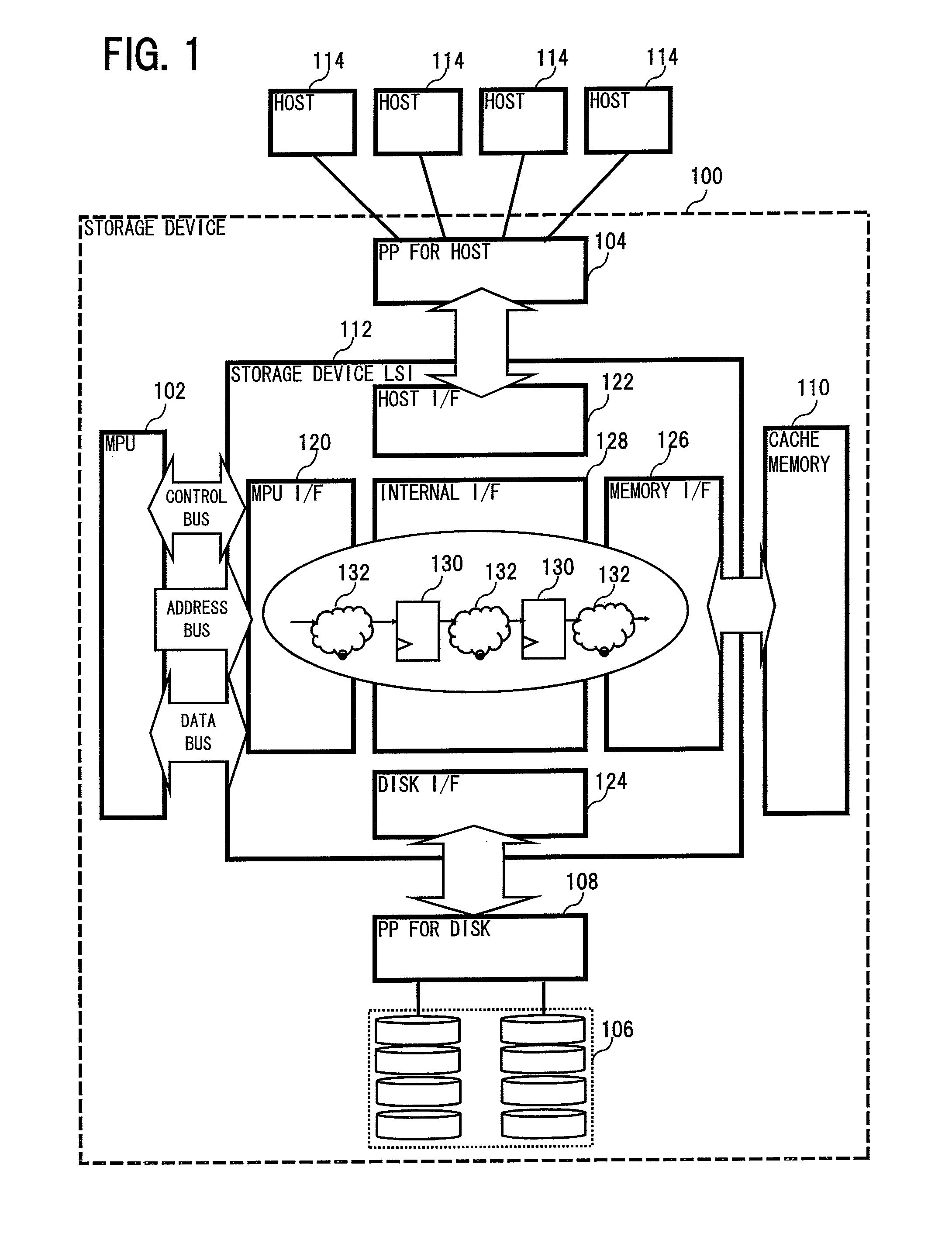
[0124]FIG. 1 shows the system structure of a storage device which is one typical example of the field of application of LSI, and which is designed with an embodiment of the LSI design apparatus according to the present invention.

[0125]The storage device 100 shown in FIG. 1 comprises an MPU 102 for controlling the storage device 100 as a whole, a protocol for host processor 104 for communicating with one or more hosts 114, a recording disk array 106 for storing data which is used by the hosts 114, a protocol for disk processor 108 for communicating with the recording disk array 106, a cache memory 110 which temporarily stores data inputted and outputted to and from the recording disk array 106, a storage device LSI 112 which functions as an interface between these devices 102, 104, 108, and 110, and the like.

[0126]The storage device LSI...


PUM


Abstract

The LSI design apparatus adds diagnostic circuitry for micro diagnosis to a behavior level description. Based on behavior level design data for a normal system of a LSI, high level synthesis generates RTL design data and register information. Based on the register information, a unique address used by a micro diagnosis program is allocated to each register. Circuit components within the normal system are grouped together. Based on the result of the address allocation and the result of the grouping, a behavior description for diagnostic circuits constituting a diagnosis system for the LSI is generated and added to the behavior level design data for the normal system, resulting in behavior level design data in which the normal and diagnosis systems are integrated together.

Description

TECHNICAL FIELD[0001]The present invention relates to an apparatus, a method, and a computer program for designing an LSI (Large Scale Integration), and for example relates to such a device, a method, and a computer program which may be applied to designing a LSI logical circuit which is used in a storage device. The present invention also relates to an LSI designed by the above apparatus and / or method.BACKGROUND ART[0002]Since a high reliability computer system, of which a storage device is representative, can be continually operated for 24 hours per day and 365 days per year, accordingly such a system is endowed with a plurality of functions for detecting any fault in the hardware which is used internally to the storage device at an early stage, in order to ensure that the storage device operates stably. For example, in relation to an LSI which performs data transfer internally in the storage device, it is known for an MPU to execute a diagnosis program for this LSI, and for a mic...

Claims


Application Information

Patent Timeline
Patent Type & Authority Patents(United States)
IPC IPC(8): G06F17/50G01R31/28
CPCG06F17/5022G06F17/505G06F2217/14G06F30/333G06F30/327G06F30/33G06F30/3308
Inventor SENO, SHUNTARO
Owner HITACHI LTD
Why Eureka
Try Eureka