ESD protection circuit for low voltages

a protection circuit and low voltage technology, applied in the direction of emergency protection arrangements for limiting excess voltage/current, pulse techniques, semiconductor/solid-state device details, etc., can solve the problem of fundamental problems such as the requirement of a large area on the part of the esd circuit, irreversible changes in its components or assemblies, and damage to the entire ic. , to achieve the effect of reducing the danger of damag

Active Publication Date: 2012-07-31
ATMEL CORP
View PDF9 Cites 5 Cited by
  • Summary
  • Abstract
  • Description
  • Claims
  • Application Information

AI Technical Summary

Benefits of technology

[0012]The second field-effect transistor can have a smaller channel area than the first field-effect transistor in order to keep the area required by the ESD protection circuit small.
[0018]The voltage dropping through this third resistance when the Zener diode breaks down reduces the voltage between a gate oxide of the control terminal and a drain terminal of the second field-effect transistor and thereby reduces the danger of damage to this gate oxide during an ESD event.

Problems solved by technology

When such discharge processes act on an integrated circuit, irreversible changes in its components or assemblies can occur, for example by burn-through of thin layers (thin-film burn-out), filamentation, and short-circuiting of layer junctions (junction spiking), charge carrier injection in oxide layers or oxide rupture, which under some circumstances leads to destruction of the entire IC.
In the general trend toward increasing packing densities of integrated circuits, a requirement on the part of the ESD circuit for a large area is fundamentally problematic.

Method used


Image

  • ESD protection circuit for low voltages
  • ESD protection circuit for low voltages
  • ESD protection circuit for low voltages

Examples


Embodiment Construction

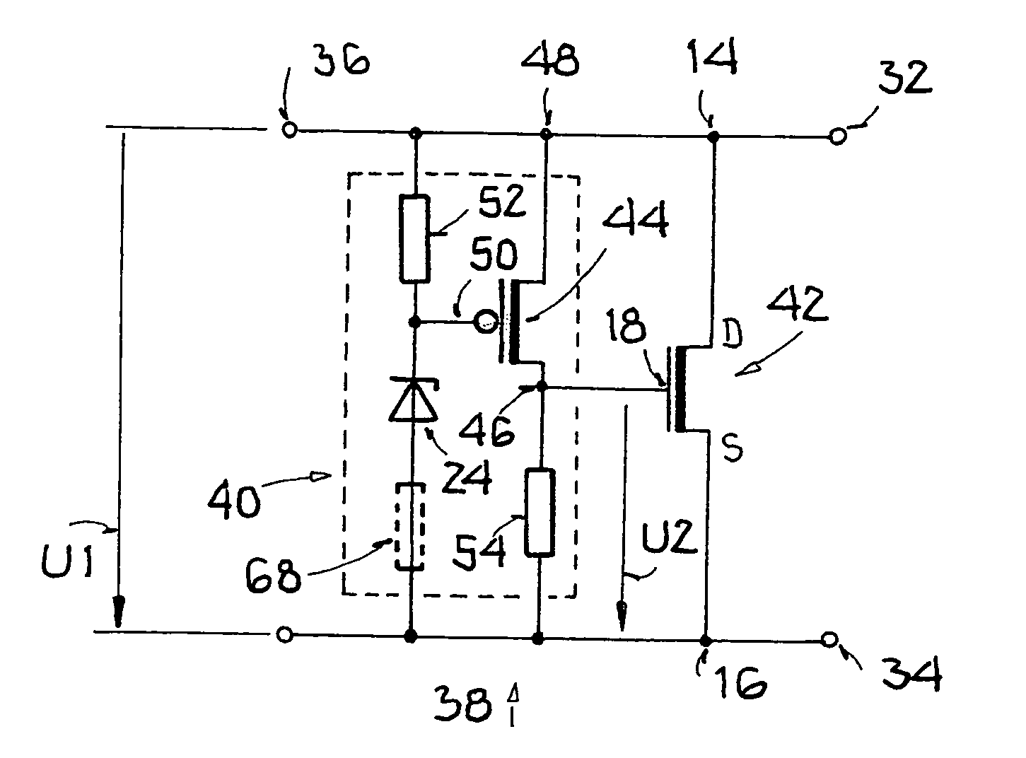
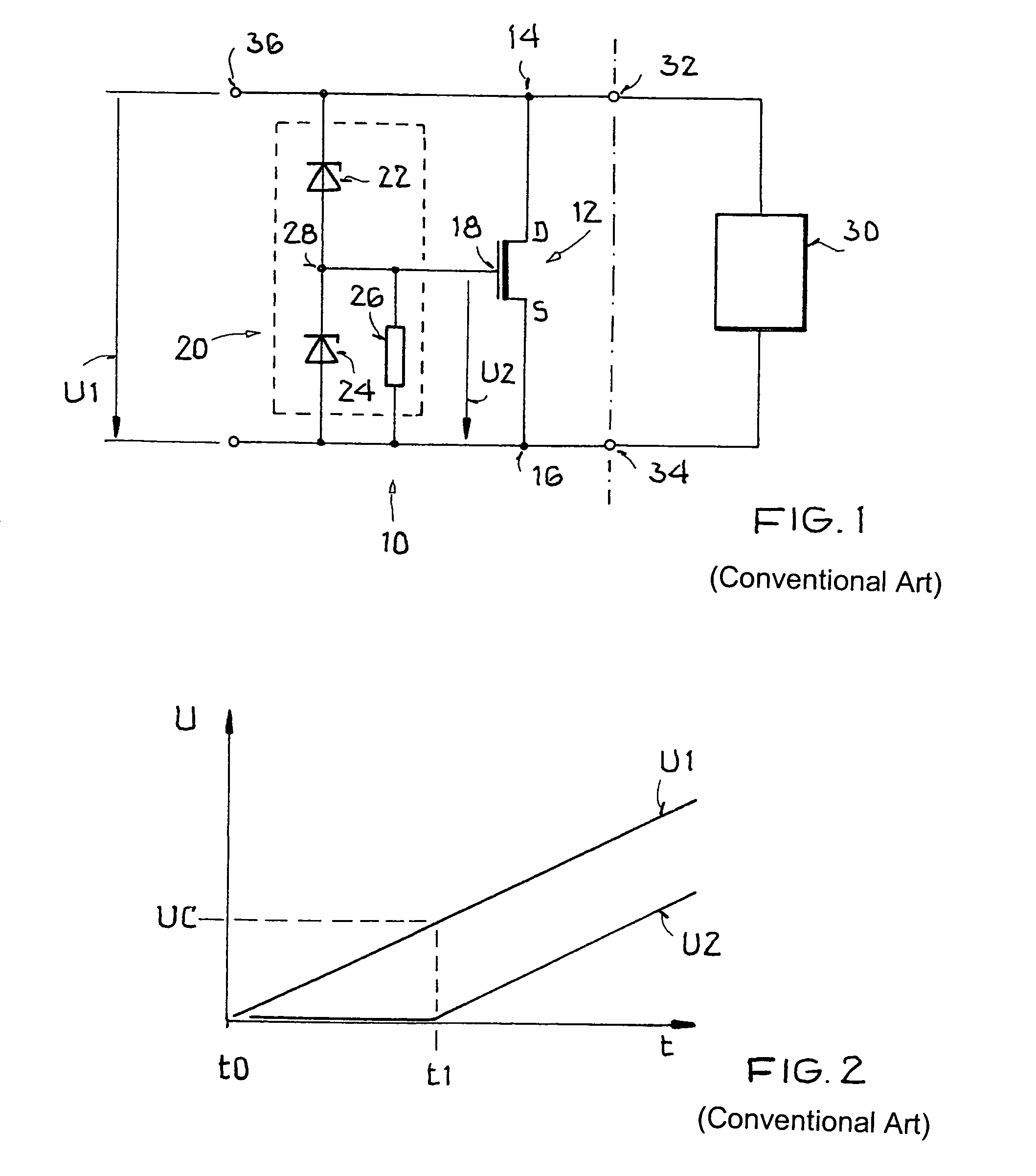
[0027]FIG. 1 shows an ESD protection circuit 10 with a first field-effect transistor 12, which has a first drain terminal 14, a first source terminal 16 and a first control terminal (gate) 18. Drain terminals (source terminals) of the first field-effect transistor are additionally labeled in the figures with D (S). A voltage U1 is present across the first field-effect transistor 12. When the voltage U1 crosses a threshold value during an ESD event, an input network 20 changes a second voltage U2 that arises between the first control terminal 18 and the first source terminal 16.

[0028]The input network 20 in the conventional ESD protection circuit consists of a series circuit of two Zener diodes 22, 24, and an ohmic resistance 26 that is connected to a center tap 28 of the series circuit. The series circuit is connected antiparallel to the first voltage U1 and thus in parallel to the channel of the first field-effect transistor 12, and the resistance 26 is also connected to the first ...


PUM


Abstract

An ESD protection circuit is provided having a first field-effect transistor, which has a first drain terminal, a first source terminal and a first control terminal, and having an input network which, in the event that a first voltage present between the first drain terminal and the first source terminal crosses a threshold value, alters a second voltage that appears between the first control terminal and the first source terminal. The input network contains a second field-effect transistor, complementary to the first field-effect transistor, having a second drain terminal, a second source terminal and a second control terminal, wherein the first drain terminal is connected to the second source terminal and, through a first resistance, to the second control terminal, and the second drain terminal is connected to the first control terminal and, through a second resistance, to the first source terminal.

Description

[0001]This nonprovisional application claims priority under 35 U.S.C. §119(a) on German Patent Application No. DE 102005013687, which was filed in Germany on Mar. 18, 2005, and which is herein incorporated by reference.BACKGROUND OF THE INVENTION[0002]1. Field of the Invention[0003]The present invention relates to an ESD protection circuit having a first field-effect transistor, which has a first drain terminal, a first source terminal and a first control terminal (gate), and having an input network which, in the event that a first voltage present between the first drain terminal and the first source terminal crosses a threshold value, alters a second voltage that appears between the first control terminal and the first source terminal.[0004]2. Description of the Background Art[0005]In the handling and use of integrated circuits (IC), it is necessary to protect the components and assemblies contained therein from the effects of overvoltages. In this context, overvoltages are defined...

Claims


Application Information

Patent Timeline
Patent Type & Authority Patents(United States)
IPC IPC(8): H02H9/00H01L23/60H01L27/02H02H9/04H03K17/082H03K17/30
CPCH01L27/0266H02H9/046H03K17/0822H03K17/302
Inventor GROMBACH, PETERKLAUSSNER, MANFRED
Owner ATMEL CORP
Why Eureka
Try Eureka