Electrical connector for circuit board

a technology of electrical connectors and circuit boards, applied in the direction of printed circuits, line/current collector details, electrical apparatus, etc., can solve the problems of difficult to meet the contradictory conditions, achieve the effect of preventing solder wicking, high solder wetting, and satisfactorily maintaining the preventive effect of solder wicking

Active Publication Date: 2012-08-07
HIROSE ELECTRIC GROUP +1
View PDF4 Cites 16 Cited by
  • Summary
  • Abstract
  • Description
  • Claims
  • Application Information

AI Technical Summary

Benefits of technology

[0016]Accordingly, at the backside section, the upper end of the low solder wetting area is set below the upper end of the contact-face section and the side-face sections, i.e., being closer to a circuit board surface to be connected by soldering. Even if the range of the low solder wetting area in the longitudinal direction is smaller, there is no solder wicking problem, and by lowering the upper end of the low solder wetting area on the backside section, the area of the contact section, which is provided thereabove, can be made broader. As a result, without interfering with the preventive effect against solder wicking on the back-face section, it is possible to enhance the secure contact with a terminal of the mating connector at the contact section. Therefore, according to the invention, it is possible to reduce the profile of a connector, and especially it is effective in a connector which is required to have lower profile.
[0019]In the invention, it is possible to form a high solder wetting area surface by gold plating and a low solder wetting area surface by nickel plating, respectively.
[0020]In the invention, it is possible to form the low solder wetting area by removing or dissolving the high solder wetting material layer by irradiation of laser beam.
[0021]According to the invention, in a terminal that has a low solder wetting area to prevent solder wicking, since the upper end of the low solder wetting area on the backside section, where a contact section is formed, is provided lower than the upper ends of the side-face sections and the contact-face section, it is possible to secure large contact section, which is above the upper end of the low solder wetting area on the backside section, and thereby each terminal can securely contact with a terminal of a mating connector.
[0022]In addition, the backside section is a surface where solder wicking occur less, and even if the upper end of the low solder wetting area is provided lower than the upper end of the contact-face section or the side-face sections, the preventive action against the solder wicking would not be impaired. On the other hand, since the upper ends of the low solder wetting areas on the contact-face section and the side-face sections, where solder wicking occurs more highly likely that the backside section, are provided higher than the upper end of the backside section and broad low solder wetting area is secured, the preventive effect against solder wicking is satisfactorily maintained.
[0023]Accordingly, not only in a connector, in which each terminal is attached to a housing while having slight space from the housing, but also in a connector, in which each terminal is integrally molded to a housing, even if there is a possibility that a connector may have space generated by peeling after molding or the like, it is possible to prevent solder wicking.

Problems solved by technology

In this circumstance, it is difficult to meet the contradictory conditions also in view of the low profile demand.

Method used


Image

  • Electrical connector for circuit board
  • Electrical connector for circuit board
  • Electrical connector for circuit board

Examples


Embodiment Construction

[0032]Referring now to the accompanying drawings, embodiments of the invention will be described.

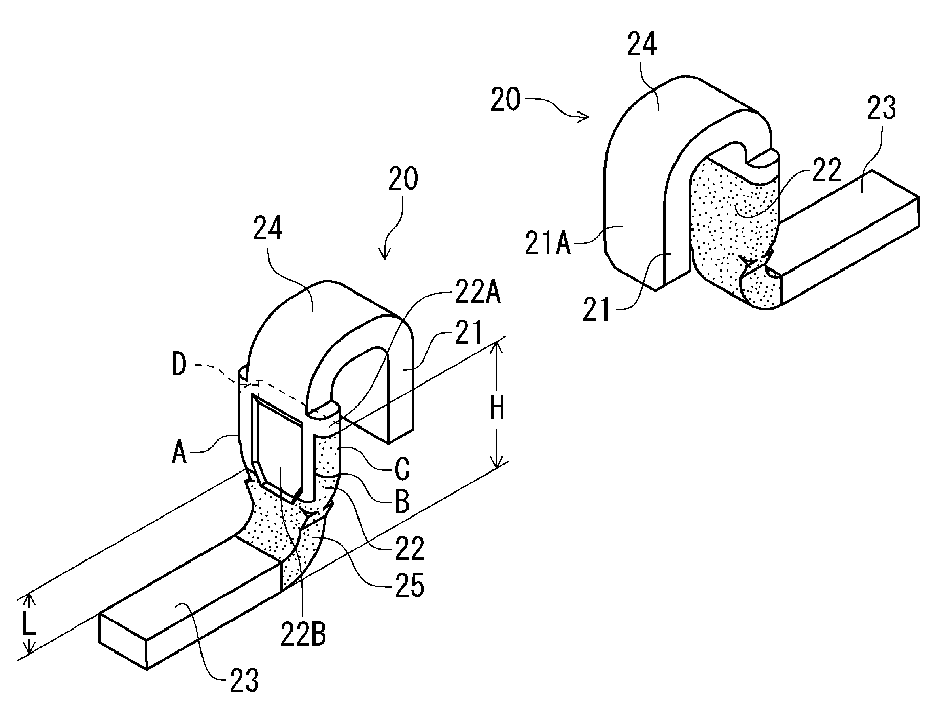
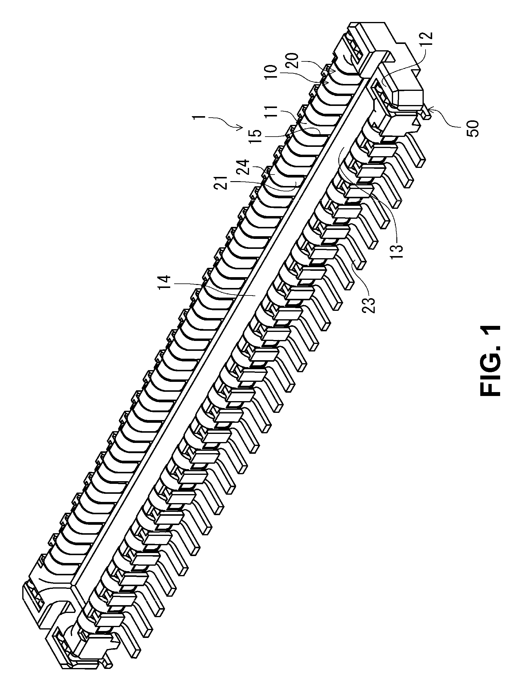
[0033]A connector 1 shown in FIG. 1 according to the embodiment has terminals 20, which are arranged and attached to a pair of side walls (wall sections) 11 that respectively extend in a longitudinal direction of a housing 10, which has a rectangular shape in the top view. In addition, the housing 10 has on its both ends in the longitudinal direction fixing brackets 50 to secure the connector 1 onto a circuit board (not illustrated).

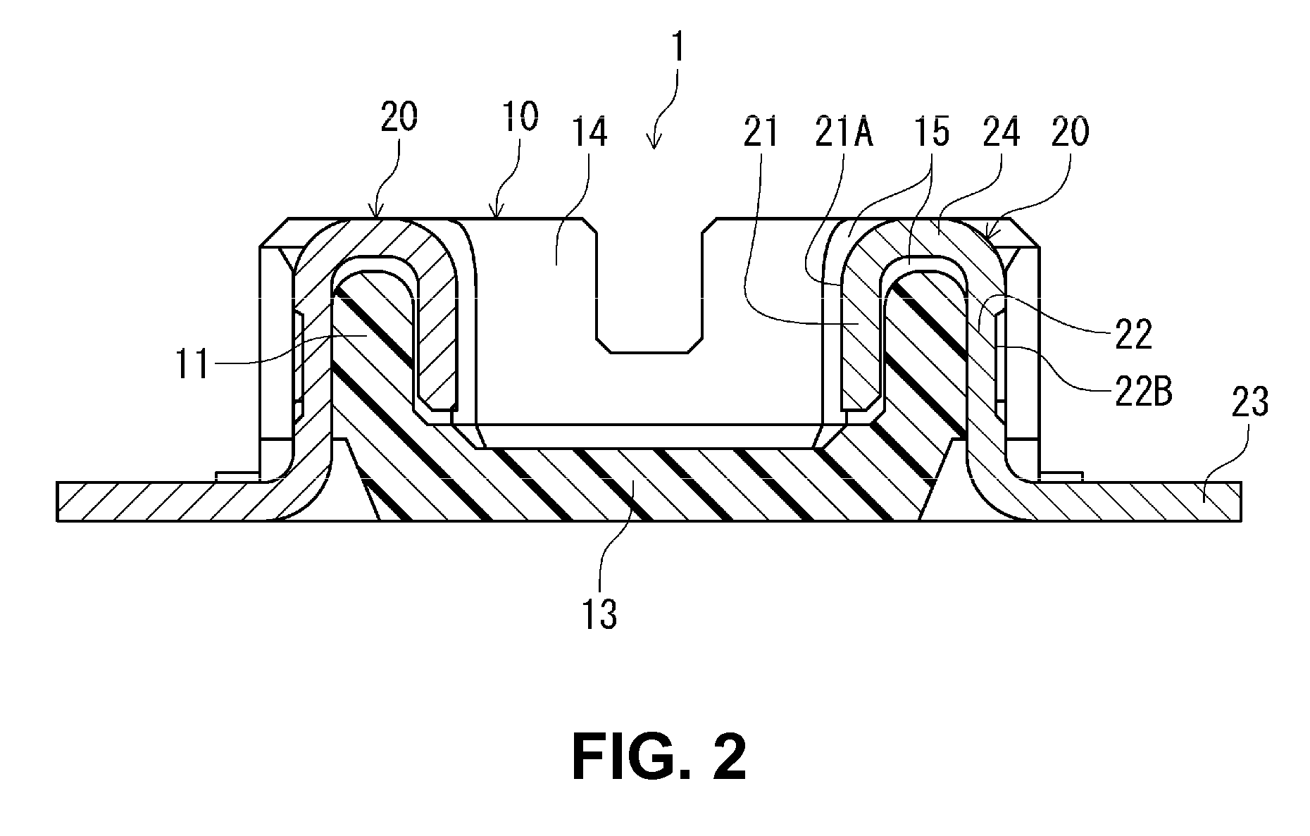
[0034]The housing 10 is made of an electrically insulating material, and has a receiving recess 14 to receive a mating connector (not illustrated), being formed by a pair of side walls 11 facing each other and extending in the longitudinal direction, end walls 12 that connect the pair of side walls 11 at the both ends in the longitudinal direction, and a bottom wall 13 provided at the lower end sides of the side walls 11 and the end walls 12.

[0035]As shown in...


PUM


Abstract

In an electrical connector to be attached to a circuit board, a terminal has a contact section on one free end side to contact with a terminal of a mating connector and has a connecting section on the other free end side to be connected by soldering to a circuit portion of a circuit board. The terminal has a holding section and a connecting section. The holding section has a face-contact section, a backside section, and a side-face section. The terminal has a low solder wetting area at least on a part of a circumferential area of the holding section in the longitudinal direction, and the contact section is formed above the upper end of the low solder wetting area on the backside section. The upper end of the low solder wetting area is provided below the upper end at the side-face sections and the contact-face section.

Description

BACKGROUND OF THE INVENTION AND RELATED ART STATEMENT[0001]The present invention relates to an electrical connector for a circuit board.[0002]An electrical connector for a circuit board is connected by soldering connecting sections of terminals of the connector to a corresponding circuit portion of a circuit board upon attaching to the circuit board. A connector of this type has been known as one disclosed in Patent Reference.[0003]Patent Reference: Japanese Patent Publication No. 2008-226681[0004]The connector of Patent Reference has a housing having a circumferential wall, which extends orthogonally to a circuit board surface to receive a mating connector, and the terminals are integrally molded onto the facing side walls of the circumferential wall. Each terminal has a contact section provided along an inner surface of the side wall and a connecting section that is bent at its end and extends outside the housing. Each terminal contacts with a terminal of a mating connector at the...

Claims


Application Information

Patent Timeline
Patent Type & Authority Patents(United States)
IPC IPC(8): H05K1/00
CPCH01R12/57H01R12/716H01R43/0256
Inventor YAMASHIRO, NAOYAMICHIDA, YOHEIOSHITA, FUMIOKATOU, TOMOAKIHAYASHI, HIROKI
Owner HIROSE ELECTRIC GROUP
Why Eureka
Try Eureka