Method of manufacturing semiconductor device

a manufacturing method and semiconductor technology, applied in the direction of semiconductor devices, basic electric elements, electrical appliances, etc., can solve the problems of difficult to obtain a gan layer having a predetermined thickness, difficult to reliably stop the cmp in a predetermined position, etc., to achieve high-precision thickness, easy and efficient fabrication

Active Publication Date: 2012-08-07
SONY CORP
View PDF3 Cites 0 Cited by
  • Summary
  • Abstract
  • Description
  • Claims
  • Application Information

AI Technical Summary

Benefits of technology

[0010]It is therefore desirable to provide a method of manufacturing a semiconductor device to efficiently manufacture a semiconductor device including a nitride semiconductor layer having high-precision thickness.
[0012]In the method of manufacturing a semiconductor device of an embodiment of the invention, a metal layer is formed so as to bury trenches in the +c face of the GaN layer. After that, the −c face of the GaN layer is entirely polished, and a part in the thickness direction of the layer is removed. By the operation, at the time point the metal layer filled at the bottom of the trenches is exposed, the polishing rate decreases largely, so that it is easier to stop the polishing process without progressing the process excessively. Alternatively, the polishing process may be performed while detecting a change in electric resistance and stopped when a sharp change in the electric resistance occurs when the metal layer is exposed. In any case, the GaN layer having a thickness according to the depth of the trench remains.
[0013]According to the method of manufacturing a semiconductor device of an embodiment of the invention, after forming the metal layer so as to bury the trenches in the +c face of the GaN layer, polishing on the −c face on the side opposite to the +c face in the GaN layer is progressed. Consequently, at the time point when the metal layer is exposed, the polishing is stopped promptly. As a result, the GaN layer having a high-precision thickness is easily and efficiently fabricated.

Problems solved by technology

However, when the CMP is performed on the −c face of the GaN layer, due to the influence of the high polishing rate, it is difficult to reliably stop the CMP in a predetermined position.
It is therefore difficult to obtain a GaN layer having a predetermined thickness.

Method used


Image

  • Method of manufacturing semiconductor device
  • Method of manufacturing semiconductor device
  • Method of manufacturing semiconductor device

Examples


embodiment

Operation and Effect of Embodiment

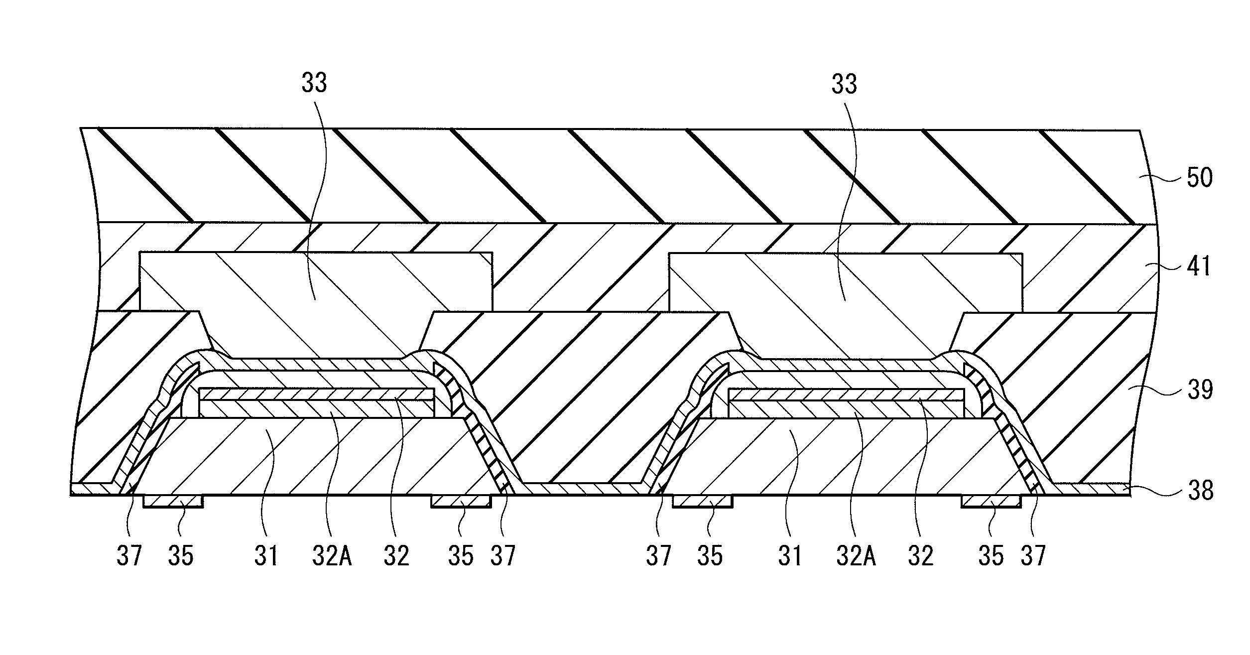
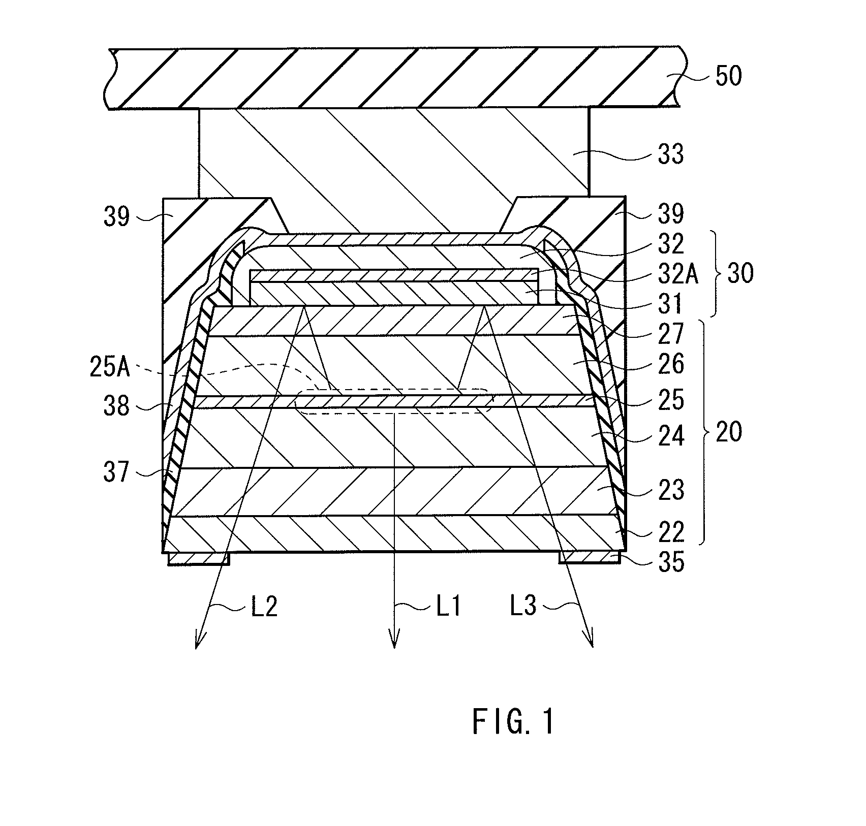
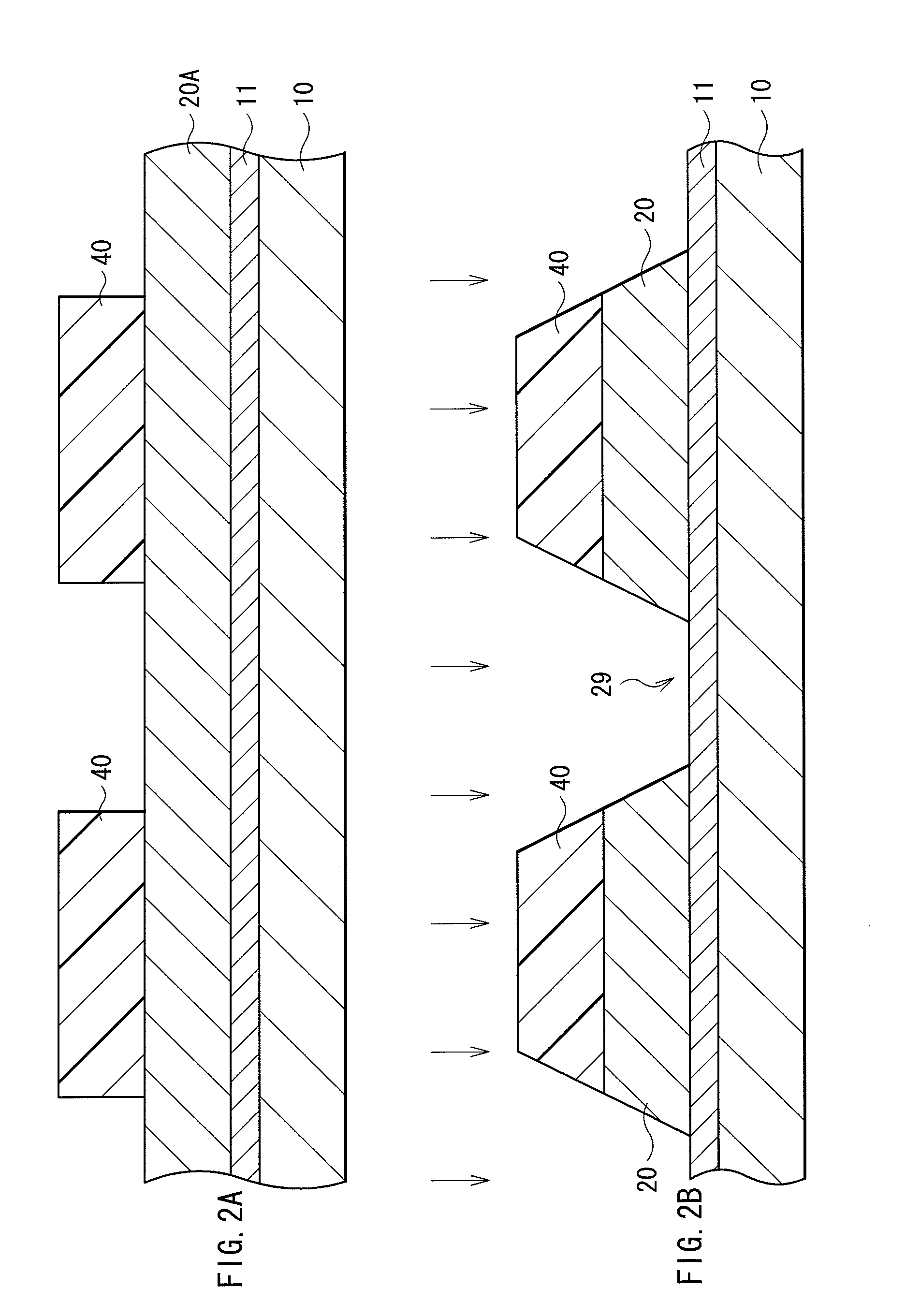
[0057]As described above, in the embodiment, a plurality of semiconductor layers 20 made of GaN or the like and separated by the trenches 29 are formed on the buffer layer 11 and, after that, the metal layer 38 is formed so as to cover the bottom faces of the trenches 29 and in contact with the +c face of the semiconductor layer 20. After that, CMP is performed from the side of the −c face of the semiconductor layer 20 to eliminate all of the buffer layer 11 and a part in the thickness direction of the semiconductor layer 20. By the CMP, the polishing rate largely drops at the time point when the metal layer 38 formed at the bottom of the trench 29 is exposed on the polish face, so that it becomes easier to stop the polishing in the predetermined position without performing the CMP excessively.

[0058]The phenomenon will be considered as follows. First, GaN as the material of the semiconductor layer 20 has a crystal field by internal polarization or t...

example

[0061]An example of the present invention will be described in detail.

[0062]As an example, according to the description of the foregoing embodiment, a light emitting diode of FIG. 1 was fabricated. First, sapphire whose main face is the c face was prepared as the substrate 10, and a film was grown on the c face at 500° C. by the MOCVD to form the buffer layer 11 of undoped GaN having a thickness of 30 nm. After that, the undoped GaN was grown on the buffer layer 11 at 1,000° C. by the ELO technique, thereby forming the GaN layer 22 having a thickness of 0.5 μm. Further, on the GaN layer 22, by MOCVD, the n-type contact layer 23, the n-type cladding layer 24, the active layer 25, the p-type cladding layer 26, and the p-type contact layer 27 were sequentially grown, thereby obtaining the semiconductor film 20A. In this case, the growth temperature for the n-type contact layer 23, the n-type cladding layer 24, the p-type cladding layer 26, and the p-type contact layer 27 was about 1,00...


PUM

PropertyMeasurementUnit
thicknessaaaaaaaaaa
thicknessaaaaaaaaaa
thicknessaaaaaaaaaa

Abstract

A method of manufacturing a semiconductor device including a nitride semiconductor layer having high-precision thickness is provided. The method includes steps of: forming a gallium nitride (GaN) layer whose main face is a +c face on a substrate; forming a trench by selectively etching down a partial region in the +c face of the GaN layer; forming a metal layer so as to bury the trench; and separating the substrate and the GaN layer, after that, polishing a −c face of the GaN layer until the metal layer is exposed, and removing a part in a thickness direction of the GaN layer.

Description

BACKGROUND OF THE INVENTION[0001]1. Field of the Invention[0002]The present invention relates to a method of manufacturing a semiconductor device including a semiconductor layer made of gallium nitride (GaN).[0003]2. Description of the Related Art[0004]Nitride semiconductor such as gallium nitride (GaN) is applied in practice to a semiconductor light emitting device such as a light emitting diode (LED) and a semiconductor device such as a high-speed transistor capable of operating at high temperature.[0005]At the time of manufacturing such a semiconductor device using the nitride semiconductor, a nitride semiconductor layer is grown to a predetermined thickness on a base-material substrate such as a sapphire substrate and, after that, the interface between the nitride semiconductor layer and the base-material substrate is peeled off, thereby obtaining a nitride semiconductor substrate. For example, the nitride semiconductor layer and the base-material substrate are separated by appl...

Claims


Application Information

Patent Timeline
Patent Type & Authority Patents(United States)
IPC IPC(8): H01L21/20
CPCH01L33/0079H01L21/30625H01L33/405H01L33/62H01L2924/0002H01L2924/00H01L33/0093
Inventor HIRAO, NAOKIMIURA, YUYA
Owner SONY CORP
Why Eureka
Try Eureka