

Semiconductor device having CMP dummy pattern
a technology of dummy pattern and semiconductors, applied in the direction of semiconductor devices, basic electric elements, electrical appliances, etc., can solve the problems of reducing the productivity of devices, increasing the dram capacity, and achieving a limitation
- Summary
- Abstract
- Description
- Claims
- Application Information
AI Technical Summary
Benefits of technology
Problems solved by technology
Method used
Image

Examples
Embodiment Construction
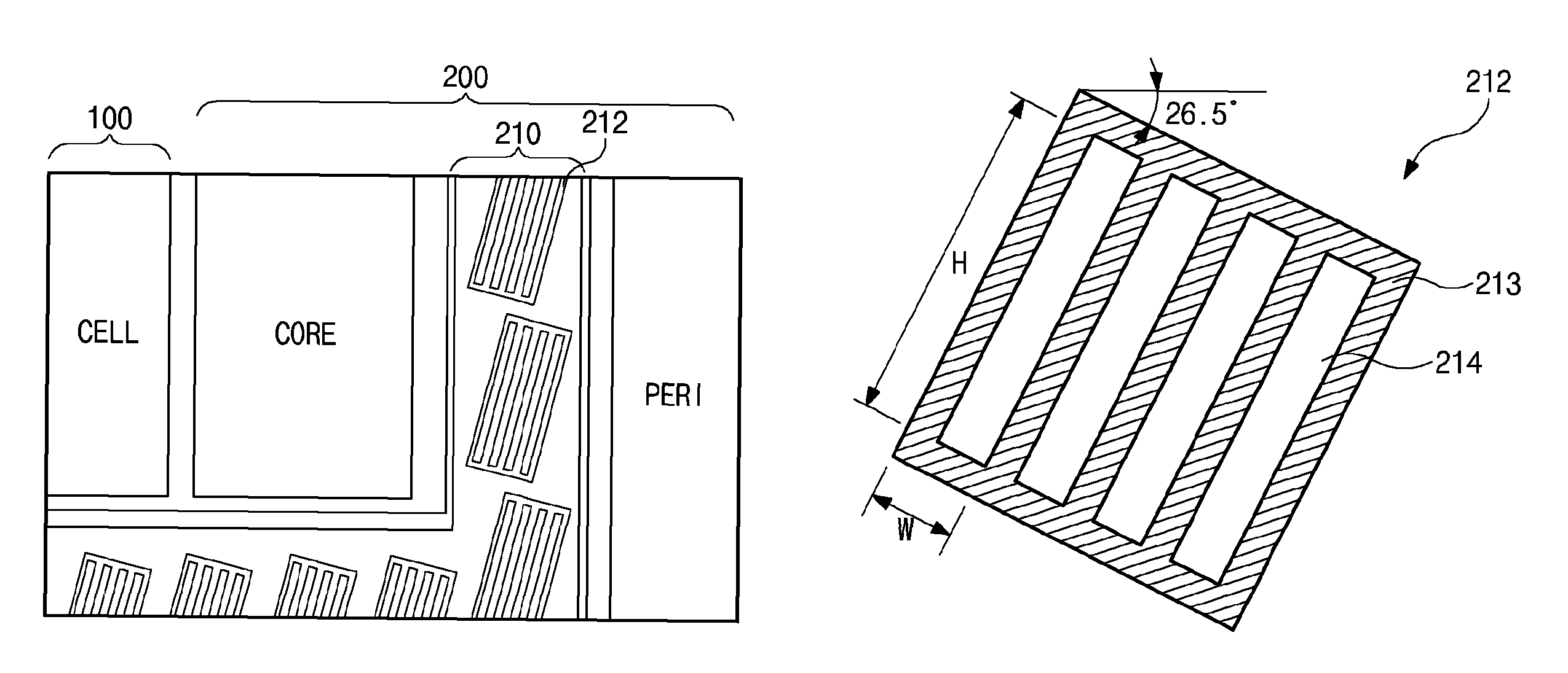
[0030]FIG. 3 is a plan view illustrating a layout of a semiconductor device having a CMP dummy pattern according to an embodiment of the present invention.
[0031]A semiconductor device is formed with a cell region 100 and a core / peripheral circuit region (hereinafter “circuit region”) 200. In a cell region 100, a density of patterns (e.g., ISO patterns or ISO structures) is high. However, in circuit region 200, a density of patterns is low and patterns have a larger width than those of the cell region 100. For convenience of explanation, a cell region 100 and a circuit region 200 in a semiconductor device having a 6F2 layout are partially illustrated in FIG. 3.
[0032]ISO patterns formed in the cell region 100 of the semiconductor device having a 6F2 layout are inclined at an angle (for example, 26.5 degrees or 116.5 degrees) in an arbitrary direction, whereas ISO patterns formed in a cell region of a semiconductor device having an 8F2 layout are arranged in a vertical direction. Howev...
PUM
 Abstract
Description
Claims
Application Information