Resistively heated small planar filament

a technology of resistive heating and planar filament, which is applied in the manufacture of electric discharge tubes/lamps, discharge tubes luminescnet screens, electrode systems, etc., can solve the problem of less performance variability between devices, and achieve the effect of improving the precision of filament placement, reducing the number of filaments, and improving the quality of filaments

Inactive Publication Date: 2012-08-21
MOXTEK INC
View PDF294 Cites 14 Cited by
  • Summary
  • Abstract
  • Description
  • Claims
  • Application Information

AI Technical Summary

Benefits of technology

[0006]It has been recognized that it would be advantageous to provide a filament which is easier to handle during manufacturing, resulting in more precise and repeatable placement of the filament. Increased precision of filament placement results in less performance variability between devices using these filaments. In addition, it has been recognized that it would be advantageous to provide a filament that maintains its shape during use and which is less susceptible to filament failures. In addition, it has been recognized that it would be advantageous to provide a smaller and more circular electron spot size in an x-ray tube. This smaller and more circular spot size can be in part the result of a filament which is manufactured and placed with high precision and a filament with a planar, rather than a helical shape.
[0007]In one embodiment, the present invention is directed to an electron emitter comprising a pair of spaced-apart bonding pads configured to receive an electrical connection and an elongated planar filament extending between the pair of bonding pads in a planar layer, the planar filament configured to receive an applied electric current therethrough. The planar filament is substantially flat with planar top and bottom surfaces. The planar filament has a length and a width in the planar layer transverse to the length. The planar filament winds in an arcuate path in the planar layer between the pair of bonding pads defining a central spiral segment with the planar filament forming at least one complete revolution about an axis at a center of the planar filament, on either side of the axis, the planar filament forming a double spiral shape oriented parallel to the layer and a pair of serpentine segments on different opposite sides of the spiral segment with each serpentine segment including at least one change in direction. The planar filament is continuous and uninterrupted across the width along an entire length of the planar filament and defines a single current path along the length between the pair of bonding pads. The planar filament has a non-uniform width measured in a plane of the layer and transverse to a length of the planar filament, including a wider, intermediate portion having a wider width that is greater than narrower portions on opposite ends of the intermediate portion, the wider width being at least twice as wide as the narrower portions, and the wider portion is disposed substantially at the axis at the center of the planar filament. This planar design allows for improved electron beam shaping. The double spiral-serpentine shape allows for improved strength and stability. The uninterrupted width, and the wider intermediate portion, allow for increased filament strength and increased lifetime.
[0008]In another embodiment, the present invention is directed to a filament device comprising a pair of spaced-apart bonding pads configured to receive an electrical connection and an elongated planar filament extending between the pair of bonding pads in a planar layer. The planar filament is substantially flat with planar top and bottom surfaces. The planar filament has a length and a width in the planar layer transverse to the length. The planar filament is continuous and uninterrupted, across the width along an entire length of the planar filament and defining a single current path along the length between the pair of bonding pads. An intermediate portion of the planar filament has a wider width that is greater than narrower portions on opposite ends of the intermediate portion, the wider width is at least two times wider than narrower portions. This planar design allows for improved electron beam, or electromagnetic radiation, shaping. The uninterrupted width, and the wider intermediate portion, allow for increased filament strength and increased filament lifetime.
[0009]In another embodiment, the present invention is directed to a filament device comprising a pair of spaced-apart bonding pads configured to receive an electrical connection and an elongated planar filament extending between the pair of bonding pads in a planar layer. The planar filament is substantially flat with planar top and bottom surfaces. The planar filament has a length and a width in the planar layer transverse to the length. The planar filament winds in an arcuate path in the planar layer between the pair of bonding pads defining a central spiral segment with the planar filament forming at least one complete revolution about an axis at a center of the planar filament, on either side of the axis, the planar filament forming a double spiral shape oriented parallel to the layer and a pair of serpentine segments on different opposite sides of the spiral segment with each serpentine segment including at least one change in direction. This planar design allows for improved electron beam, or electromagnetic radiation, shaping. The double spiral-serpentine shape allows for improved strength and stability.
[0010]In one embodiment, the above various planar filaments or electron emitters can be disposed on a support base. The support base can allow for easier and more repeatable placement onto a cathode of an x-ray tube.

Problems solved by technology

Increased precision of filament placement results in less performance variability between devices using these filaments.

Method used


Image

  • Resistively heated small planar filament
  • Resistively heated small planar filament
  • Resistively heated small planar filament

Examples


Embodiment Construction

[0027]Reference will now be made to the exemplary embodiments illustrated in the drawings, and specific language will be used herein to describe the same. It will nevertheless be understood that no limitation of the scope of the invention is thereby intended. Alterations and further modifications of the inventive features illustrated herein, and additional applications of the principles of the inventions as illustrated herein, which would occur to one skilled in the relevant art and having possession of this disclosure, are to be considered within the scope of the invention.

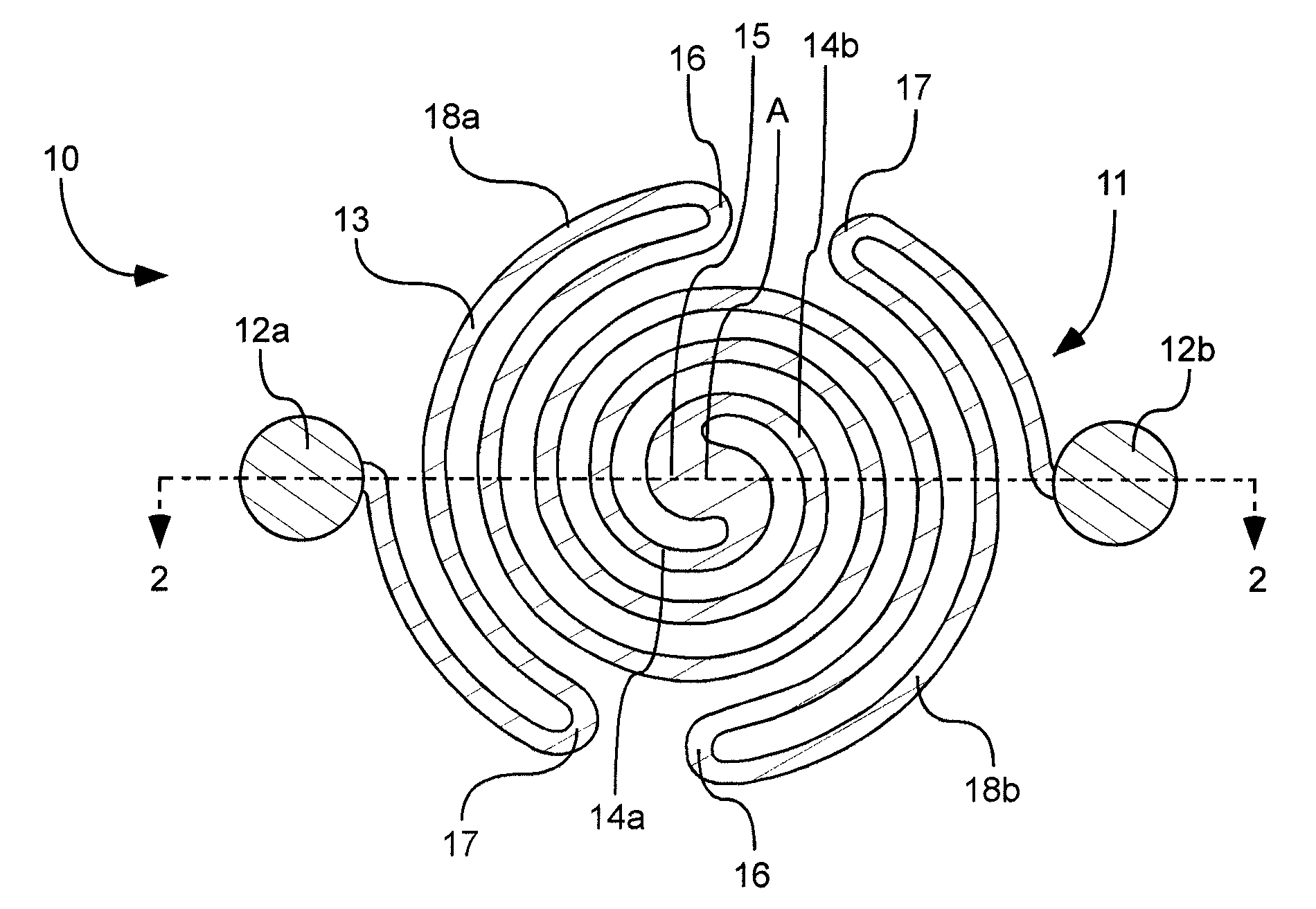
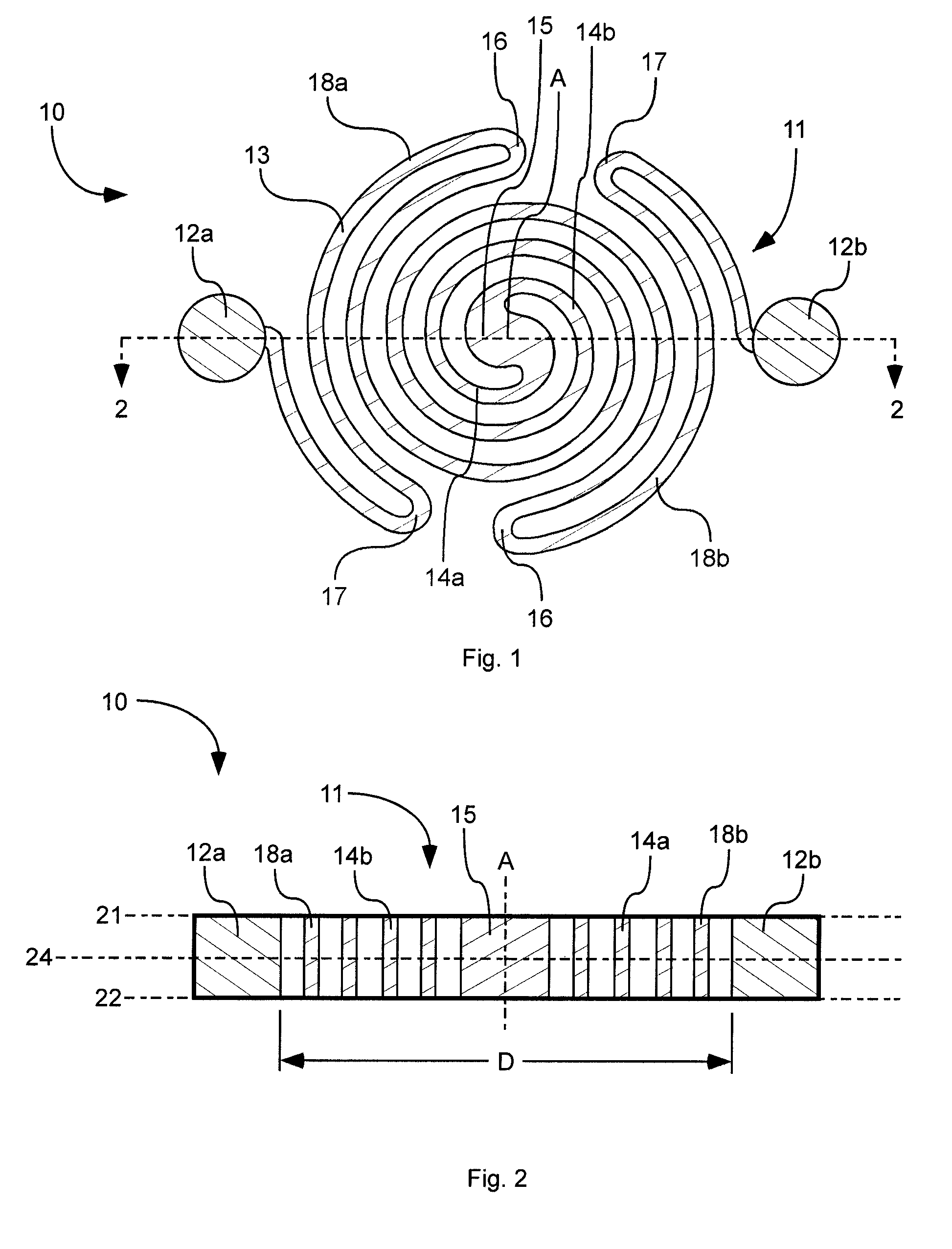
[0028]As shown in FIGS. 1-3, an electron emitter or filament device 10 is shown comprising a pair of spaced-apart bonding pads 12a-b and an elongated planar filament 11 extending between the pair of bonding pads 12a-b in a planar layer. The bonding pads 12a-b are configured to receive an electrical connection, such as being made of a shape and material that will allow for an electrical connection. The planar fila...


PUM


Abstract

A planar filament comprising two bonding pads and a non-linear filament connected between the two bonding pads. The planar filament may be wider in the center to increase filament life. The planar filament can form a double spiral-serpentine shape. The planar filament may be mounted on a substrate for easier handling and placement. Voltage can be used to create an electrical current through the filament, and can result in the emission of electrons from the filament. The planar filament can be utilized in an x-ray tube.

Description

CLAIM OF PRIORITY[0001]This is a continuation-in-part of U.S. patent application Ser. No. 12 / 407,457, filed on Mar. 19, 2009, which is hereby incorporated herein by reference in its entirety.BACKGROUND[0002]Filaments are used to produce light and electrons. For example, in an x-ray tube, an alternating current can heat a wire filament formed in a coiled cylindrical or helical loop. Due to the high temperature of the filament, and due to a large bias voltage between the filament and an anode, electrons are emitted from the filament and accelerated towards the anode. These electrons form an electron beam. The location where the electron beam impinges on the anode is called the “electron spot.” It can be desirable that this spot be circular with a very small diameter. It can be desirable that this spot be in the same location on the anode in every x-ray tube that is manufactured.[0003]The shape and placement of the filament in the x-ray tube affects the shape of the spot. Some filament...

Claims


Application Information

Patent Timeline
Patent Type & Authority Patents(United States)
IPC IPC(8): H01J17/04
CPCH01J1/16H01J1/18H01J35/06H01K1/14H01J2201/2857H01J2201/2871H01J35/064
Inventor BARD, ERIK C.CORNABY, STERLING W.
Owner MOXTEK INC
Why Eureka
Try Eureka