Inductance component
a technology of components and components, applied in the direction of inductances, transformers/inductance coils/windings/connections, inductances/transformers/magnets, etc., can solve the problems of low reliability and low reliability, and achieve high reliability, increase saturation magnetic flux, and improve magnetic permeability
- Summary
- Abstract
- Description
- Claims
- Application Information
AI Technical Summary
Benefits of technology
Problems solved by technology
Method used
Image
Examples
first embodiment
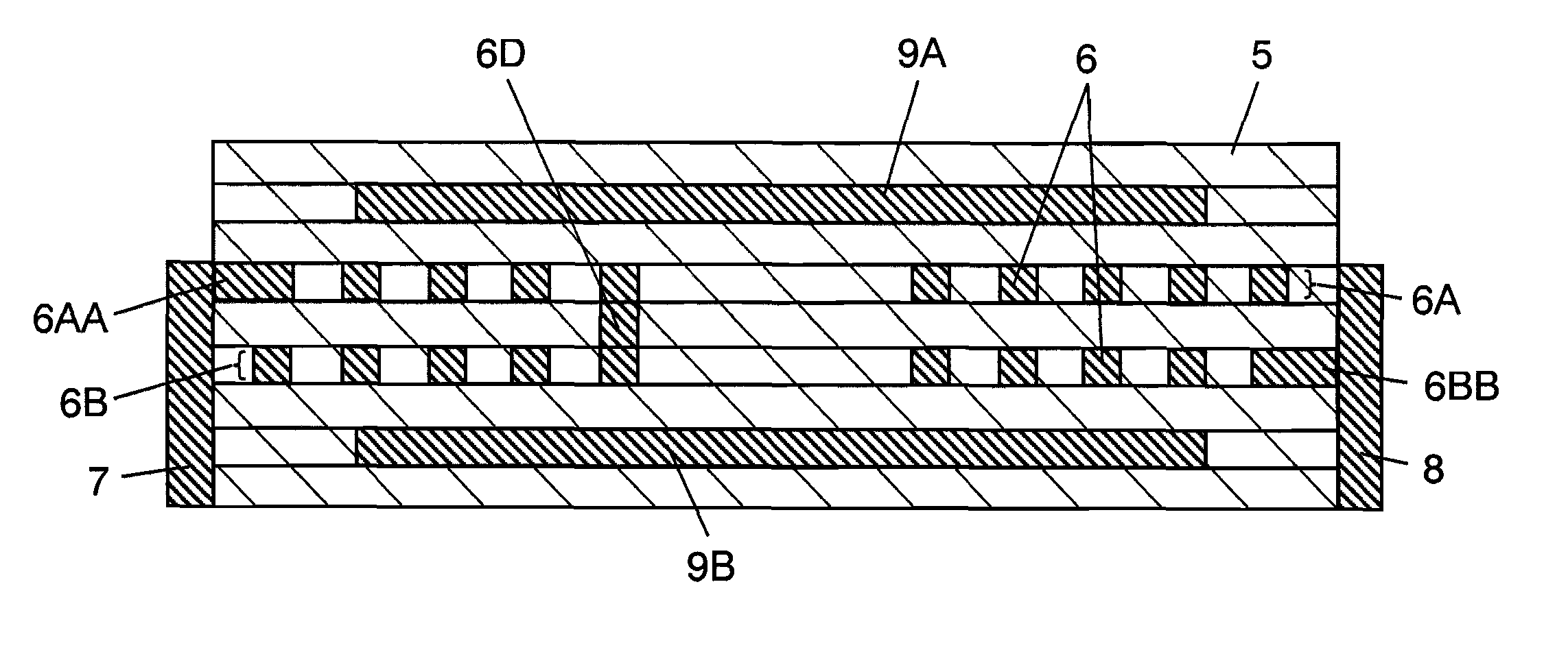
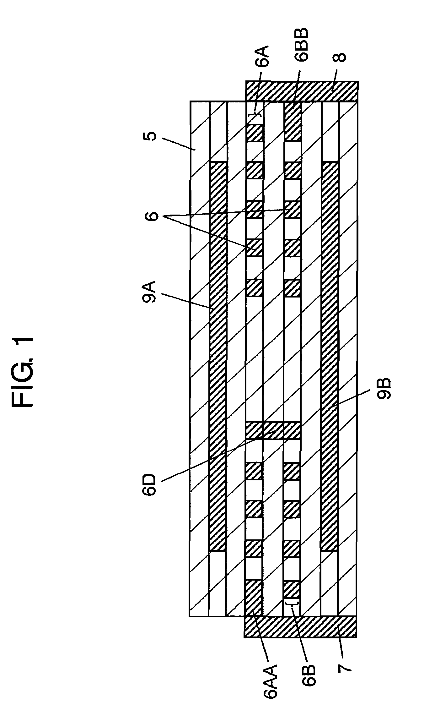
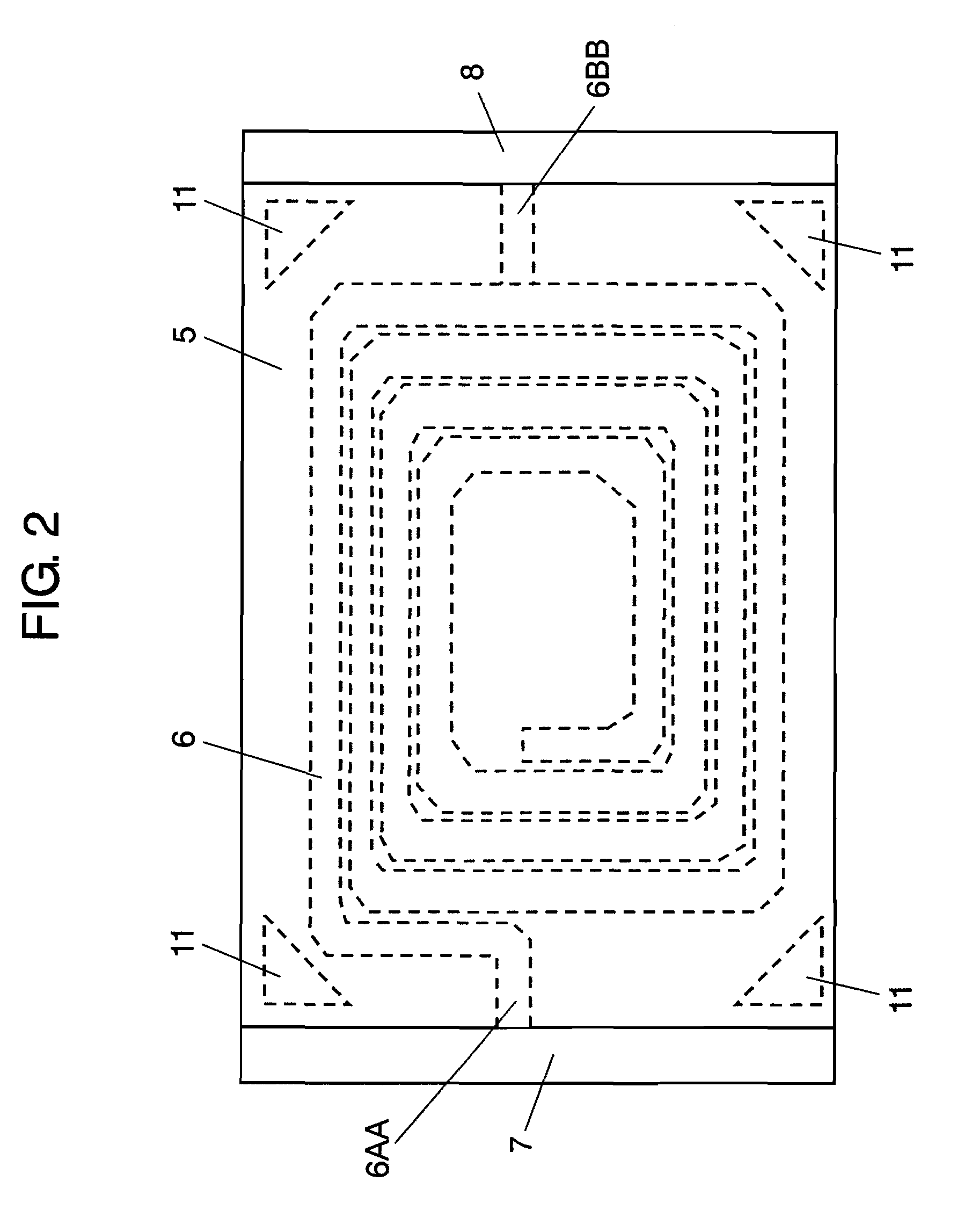
[0041]Hereinafter, an inductance component according to a first embodiment of the present invention is described with reference to FIG. 1 showing a cross-sectional view of the inductance component according to the first embodiment of the present invention, FIG. 2 showing a top view of the inductance component and FIG. 3 showing an exploded perspective view of the inductance component.
[0042]In FIG. 1, coil 6 is formed in sheet-shaped element 5, and terminals 7 and 8 are formed on an outer side of this coil 6, as shown in FIG. 2. As shown in FIG. 1, via 6D is formed between planar coils 6A and 6B, which form coil 6, in element 5, and magnetic layers 9A and 9B are formed on upper and lower sides of coil 6, respectively, in element 5.
[0043]Here, magnetic layers 9A and 9B are arranged so as to be substantially parallel to a winding surface of coil 6. This is in order to arrange magnetic layers 9A and 9B having high magnetic permeability in the path of a magnetic flux generated from coil ...
second embodiment
[0068]Next, an inductance component according to a second embodiment of the present invention is described with reference to the drawings. FIG. 5 is a cross-sectional view of the inductance component according to the second embodiment of the present invention.
[0069]In FIG. 5, coil 6 is formed in sheet-shaped element 5, terminals 7 and 8 are formed on an outer portion of this coil 6, and via 6D is formed between planar coils 6A and 6B, which form coil 6, in element 5. Portions of terminals 7 and 8 are formed of magnetic terminals 7A and 8A formed of a magnetic body.
[0070]Here, it is preferred that a metal magnetic material containing Fe or an Fe-alloy is used as a material of magnetic terminals 7A and 8A from the viewpoint of magnetic flux density and magnetic loss. In the case where Fe-alloy is used as magnetic terminals 7A and 8A, it is preferred to make the composition ratio of Fe not less than 30 percent by mass. This is because the magnetic characteristic of high saturation magn...
third embodiment
[0083]Hereinafter, an inductance component according to a third embodiment of the present invention is described with reference to the drawings. FIG. 7 is a cross-sectional view of the inductance component according to the third embodiment of the present invention.
[0084]In FIG. 7, coil 27 is formed in sheet-shaped element 26, terminals 28 and 29 are formed on outermost peripheral portions of this coil 27, and via 27C is formed between planar coils 27A and 27B, which form coil 27, in element 26.
[0085]Magnetic layers 30A and 30B, and 30C and 30D are formed on upper and lower sides of coil 27 in element 26, respectively.
[0086]Portions of terminals 28 and 29 are formed of magnetic terminals 28A and 29A formed of a magnetic body.
[0087]Further, in the present embodiment, magnetic terminals 28A and 29A in terminals 28 and 29 are formed also on the upper and lower surfaces of element 26.
[0088]On an inner portion of coil 27 in element 26, magnetic center core 31 formed of a magnetic body is ...
PUM
| Property | Measurement | Unit |
|---|---|---|
| thickness | aaaaa | aaaaa |
| particle diameter | aaaaa | aaaaa |
| particle diameter | aaaaa | aaaaa |
Abstract
Description
Claims
Application Information


