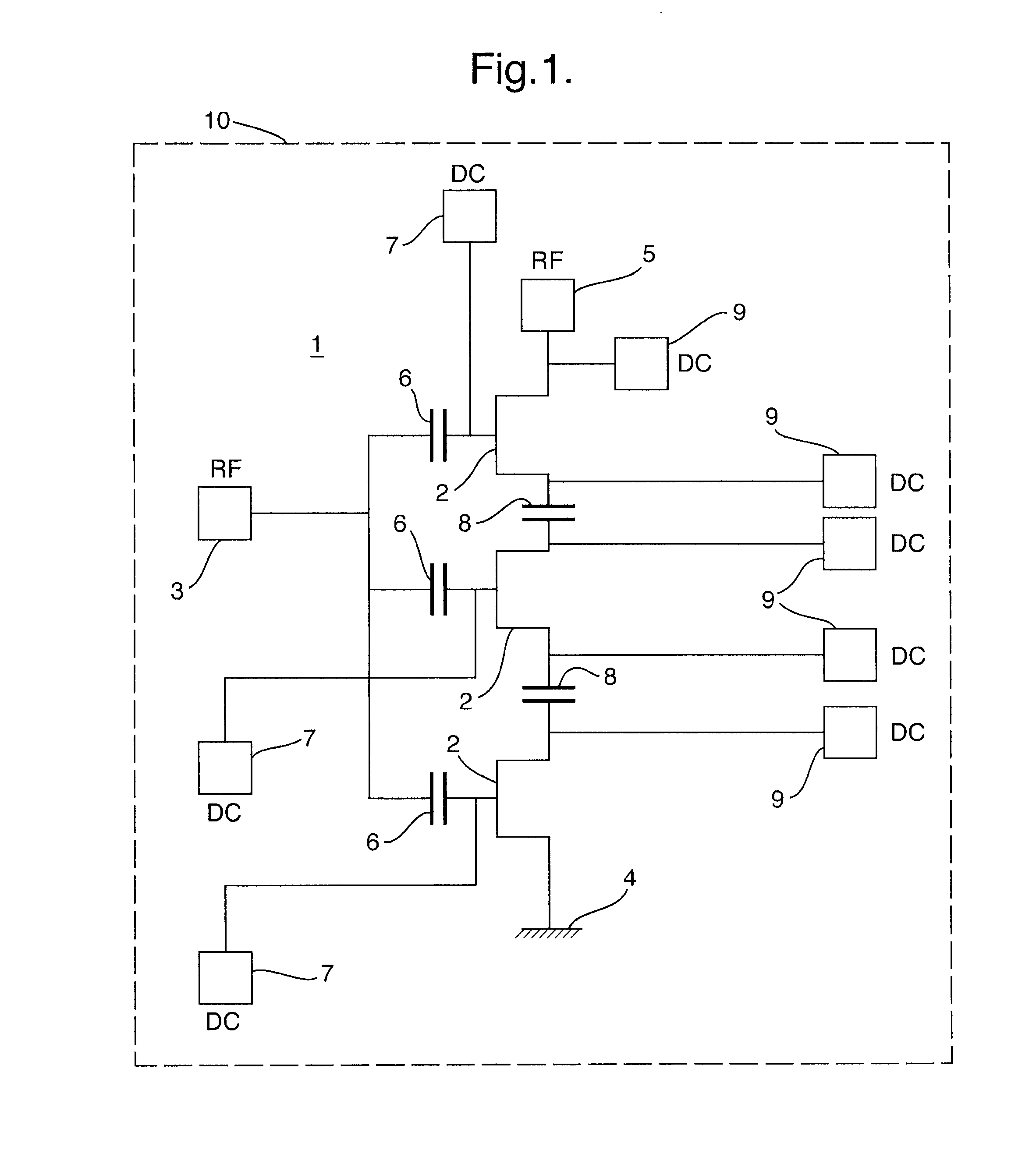
[0020]In addition, an intermediate coupling capacitor is connected between the output terminals of each adjacent pair of power amplified devices in the series stack. This is for providing DC isolation of the power amplifier devices. Consequently, the output terminals of each power amplified device are connected to respective DC voltage supply lines. The DC isolation provided by the intermediate coupling capacitors allows a separate DC bias voltage supply to be provided for each power amplifier device. This means that a DC bias voltage of a reduced level is required as compared to a series stack without intermediate coupling capacitors, as in Clifton et al. This reduced requirement for the DC bias voltage is advantageous. In many practical embodiments, this allows the power amplifier to be operated from batteries without the need for a DC-DC converter, which reduces the cost and complexity of the power amplifier, whilst still providing the operational advantages from the use of a series stack of power amplifier devices.
[0022]Such selective shorting out of one or more of the power amplifier devices allows the power amplifier to accommodate variation in the output voltage of a power supply such as a battery, in particular the discharge characteristic over the discharge thereof. In particular, the number of power amplifier devices shorted out may be higher when the voltage is high and may be reduced to introduce more power amplifier devices when the DC supply voltage reduces. By way of example, in order to provide nominal overall voltage of 7V in a power amplifier consisting of a series stack of three transistors, if the power supply voltage is greater than 3.5V then a single power amplifier device may be shorted out and when the output voltage of the power supply reduces below 3.5V, then no power amplifier devices may be shorted out.
[0023]Such shorting out of power amplifier devices allows the overall efficiency to be improved because the individual power amplifier devices may be operated with generally smaller excess bias voltages. It is also possible to use a power supply, such as a battery, along a greater portion of the discharge characteristic to a lower final voltage before the battery is considered to be discharged. This improves the effective battery life.
[0030]In addition, an intermediate coupling capacitor is connected between the output terminals of each adjacent pair of power amplified devices in the series stack. This is for providing DC isolation of the power amplifier devices. Consequently, the output terminals of each power amplified device are connected to respective DC voltage supply lines. The DC isolation provided by the intermediate coupling capacitors allows a separate DC bias voltage supply to be provided for each power amplifier device. This means that a DC bias voltage of a reduced level is required as compared to a series stack without intermediate coupling capacitors, as in Clifton et al. This reduced requirement for the DC bias voltage is advantageous. In many practical embodiments, this allows the power amplifier to be operated from batteries without the need for a DC-DC converter, which reduces the cost and complexity of the power amplifier, whilst still providing the operational advantages from the use of a series stack of power amplifier devices.
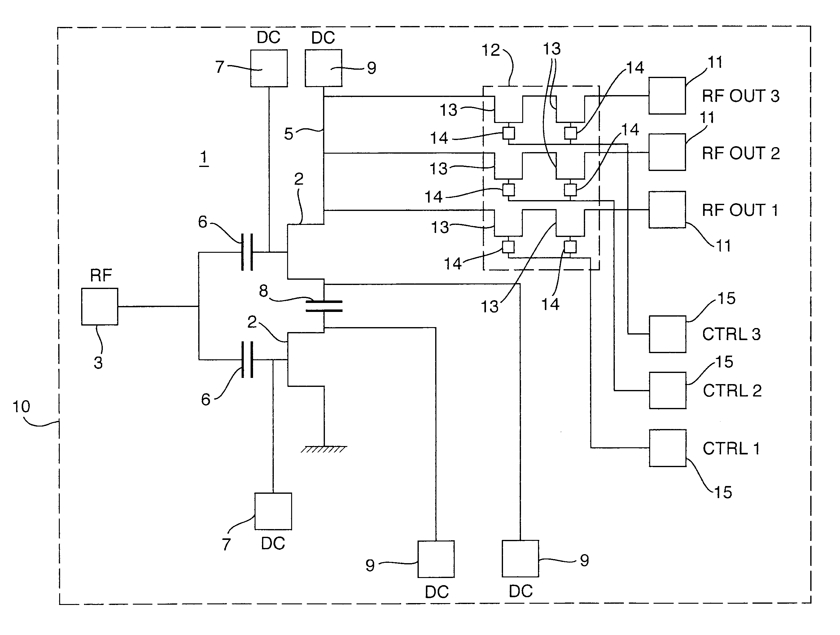
[0034]However, it has been appreciated that the relatively high output impedance of the power amplifier comprising a stack of series power amplifier devices in accordance of the present invention allows the transmit multi-through switch arrangement to be connected between the amplifier output and the plural amplifier output channels that are provided for supplying amplified RF output signals of different frequencies to respective impedance matching circuits. In other words, the design of the power amplifier allows the transmit multi-through switch arrangement to be connected upstream of the power amplifier devices.
[0035]One advantage of this is that it allows the power amplifier including the transmit multi-through switch arrangement to be formed in a single integrated circuit chip, without the need to provide the transmit multi-through switch arrangement in a separate component. This reduces the complexity of the circuitry.

