Microwave anneal of a thin lamina for use in a photovoltaic cell

a technology of photovoltaic cells and thin semiconductor laminas, which is applied in the field of microwave energy to anneal thin semiconductor laminas for use in photovoltaic cells, can solve problems such as difficulties in thermal anneal

Inactive Publication Date: 2012-09-04
NEUTRON THERAPEUTICS LLC
View PDF6 Cites 12 Cited by
  • Summary
  • Abstract
  • Description
  • Claims
  • Application Information

AI Technical Summary

Problems solved by technology

In some circumstances, however, a thermal anneal may present difficulties, as when other materials are present that cannot tolerate the anneal temperature.

Method used


Image

  • Microwave anneal of a thin lamina for use in a photovoltaic cell
  • Microwave anneal of a thin lamina for use in a photovoltaic cell
  • Microwave anneal of a thin lamina for use in a photovoltaic cell

Examples


example

Activate Dopants

[0058]Other embodiments may include a shallow junction formed at the cleaved surface, as described by Hilali et al., U.S. patent application Ser. No. 12 / 399,065, “Photovoltaic Cell Comprising an MIS-Type Tunnel Diode,” filed Mar. 6, 2009, owned by the assignee of the present application and hereby incorporated by reference.

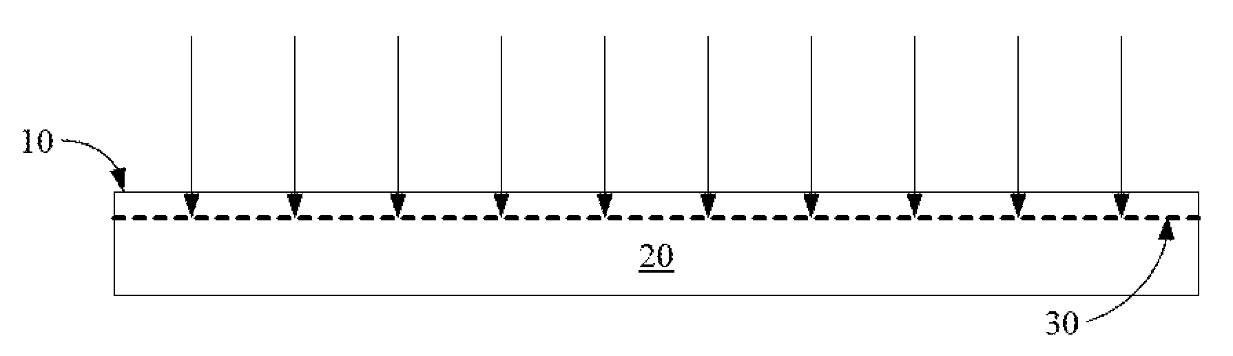
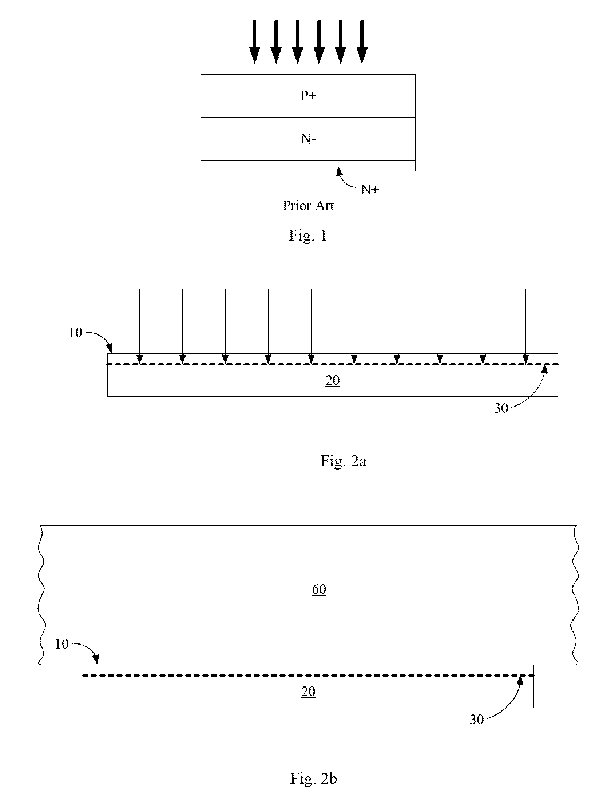
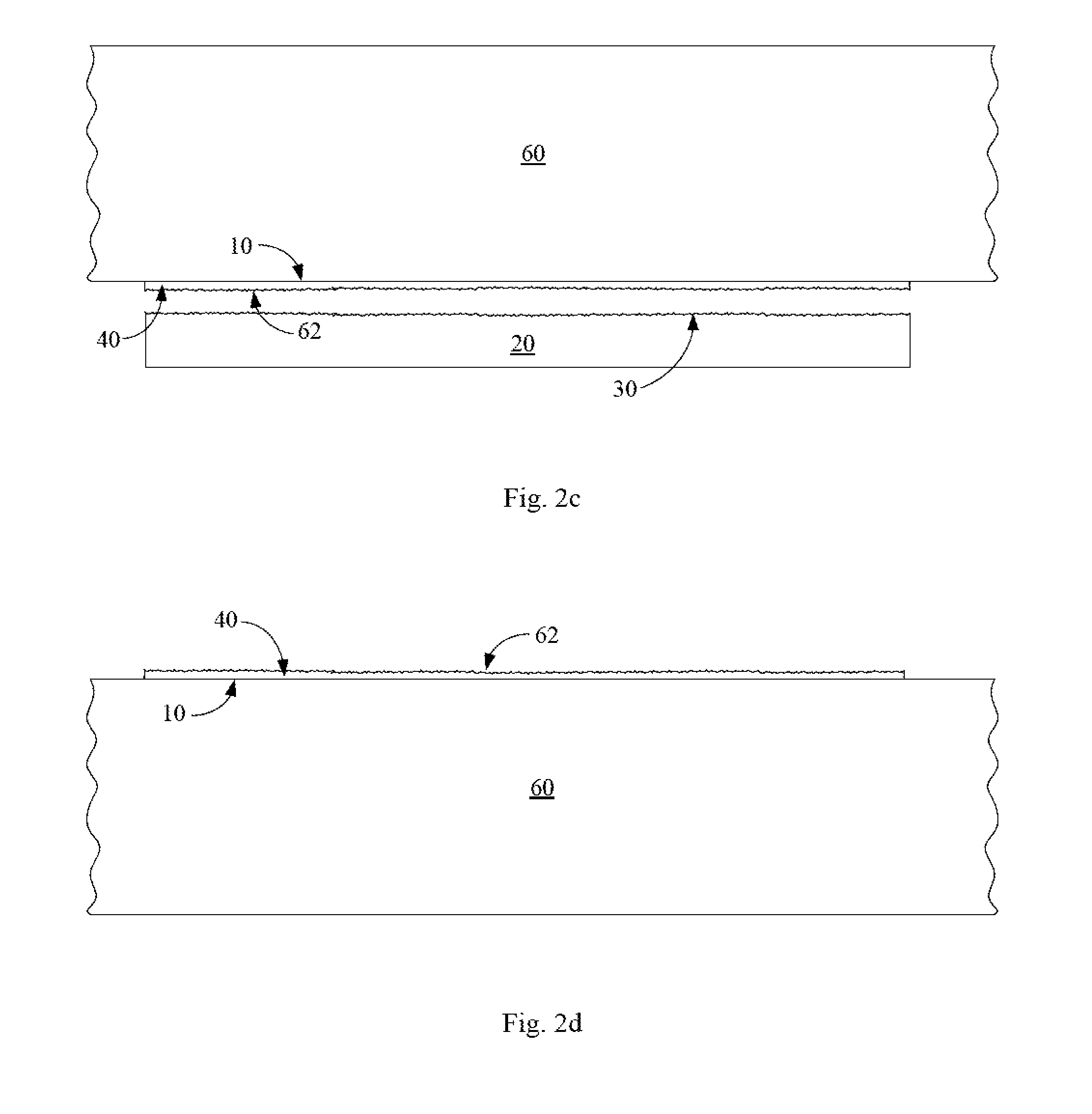
[0059]Such a shallow junction can be formed using a microwave anneal. Referring to FIG. 7, following formation of lamina 40 affixed to receiver element 60 (interposed layers, if any, are not shown), and treatment of second surface 62 to remove surface damage, a spin-on or spray-on dopant can be formed on second surface 62, including an n-type or p-type dopant, or a dopant may be provided by shallow ion implantation. A microwave anneal drives the dopant into second surface 62 of lamina 40 and activates it, forming shallow doped region 16. Fabrication continues to form a photovoltaic cell, as described by Hilali et al.


PUM


Abstract

A cleave plane is defined in a semiconductor donor body by implanting ions into the wafer. A lamina is cleaved from the donor body, and a photovoltaic cell is formed which comprises the lamina. The implant may cause some damage to the crystal structure of the lamina. This damage can be repaired by annealing the lamina using microwave energy. If the lamina is bonded to a receiver element, the receiver element may be either transparent to microwaves, or may reflect microwaves, while the semiconductor material absorbs the microwaves. In this way the lamina can be annealed at high temperature while the receiver element remains cooler.

Description

BACKGROUND OF THE INVENTION[0001]The invention relates to a method to use microwave energy to anneal a thin semiconductor lamina for use in a photovoltaic cell.[0002]Crystalline damage in semiconductor material such as silicon can be repaired by various means. One of the simplest ways is to subject the silicon body to a high-temperature anneal. In some circumstances, however, a thermal anneal may present difficulties, as when other materials are present that cannot tolerate the anneal temperature.SUMMARY OF THE PREFERRED EMBODIMENTS[0003]The present invention is defined by the following claims, and nothing in this section should be taken as a limitation on those claims. In general, the invention is directed to a method to anneal a semiconductor lamina using microwave energy.[0004]A first aspect of the invention provides for a method to form a photovoltaic cell, the method comprising the steps of: providing a semiconductor lamina bonded to a receiver element, the lamina having a firs...

Claims


Application Information

Patent Timeline
Patent Type & Authority Patents(United States)
IPC IPC(8): H01L21/00H01L21/30H01L21/46H01L21/78H01L21/301
CPCH01L21/324H01L31/068H01L31/0747H01L31/1864H01L31/056H01L31/1892H01L31/1872Y02E10/52Y02E10/547Y02P70/50
Inventor HILALI, MOHAMED MMURALI, VENKATESANPRABHU, GOPALLI, ZHIYONG
Owner NEUTRON THERAPEUTICS LLC
Why Eureka
Try Eureka