Three-dimensional macro-chip including optical interconnects

a macro-chip and optical interconnect technology, applied in the field of multi-chip modules (mcm), can solve the problems of form factor, cost, performance and cost of mcm b>100/b>, and achieve the effect of reducing manufacturing time and expens

a macro-chip and optical interconnect technology, applied in the field of multi-chip modules (mcm), can solve the problems of form factor, cost, performance and cost of mcm b>100/b>, and achieve the effect of reducing manufacturing time and expens

US8267583B2Active Publication Date: 2012-09-18ORACLE INT CORP

Image

  • Three-dimensional macro-chip including optical interconnects
  • Three-dimensional macro-chip including optical interconnects
  • Three-dimensional macro-chip including optical interconnects

Examples


Embodiment Construction

[0035]The following description is presented to enable any person skilled in the art to make and use the disclosure, and is provided in the context of a particular application and its requirements. Various modifications to the disclosed embodiments will be readily apparent to those skilled in the art, and the general principles defined herein may be applied to other embodiments and applications without departing from the spirit and scope of the present disclosure. Thus, the present disclosure is not intended to be limited to the embodiments shown, but is to be accorded the widest scope consistent with the principles and features disclosed herein.

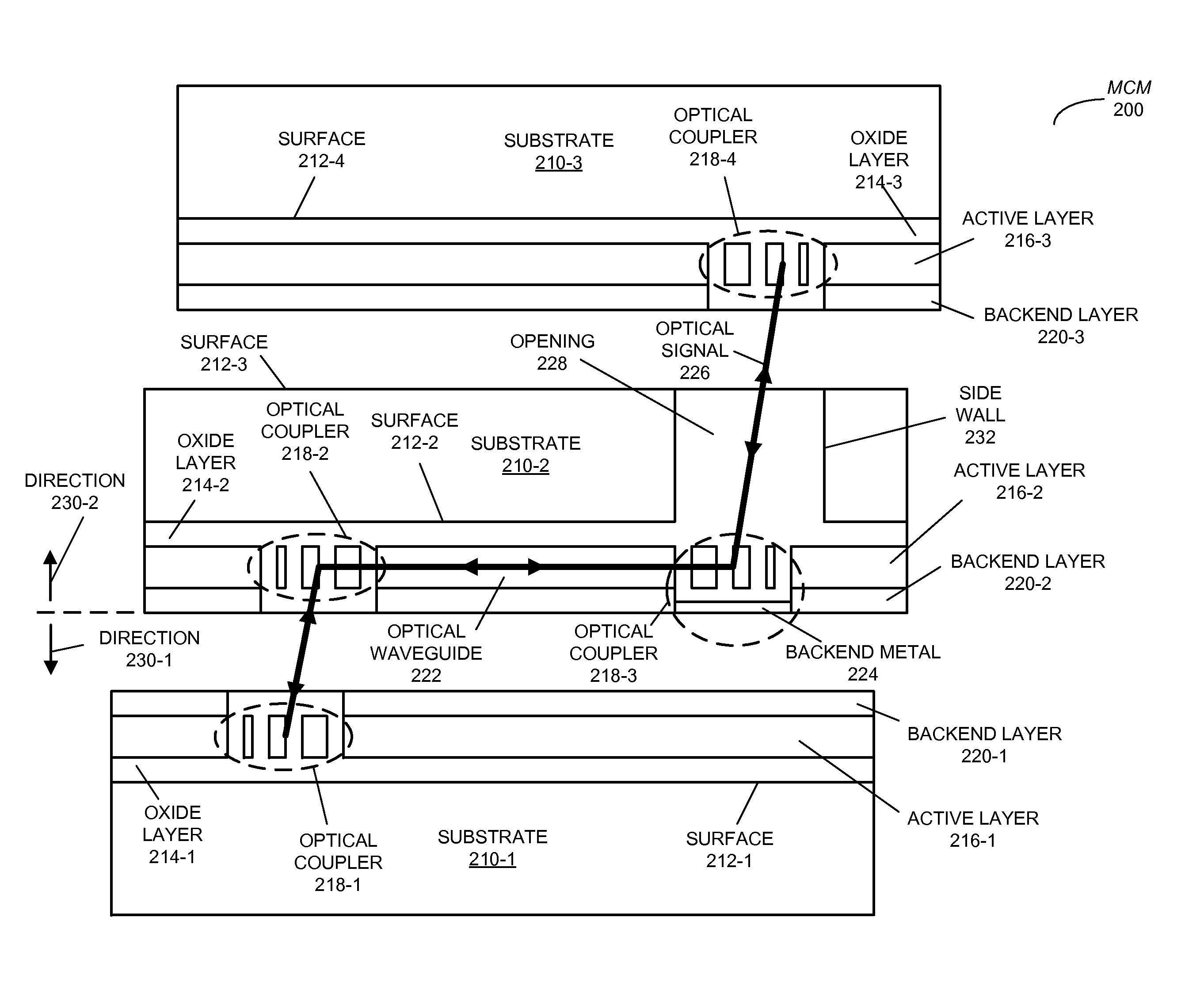
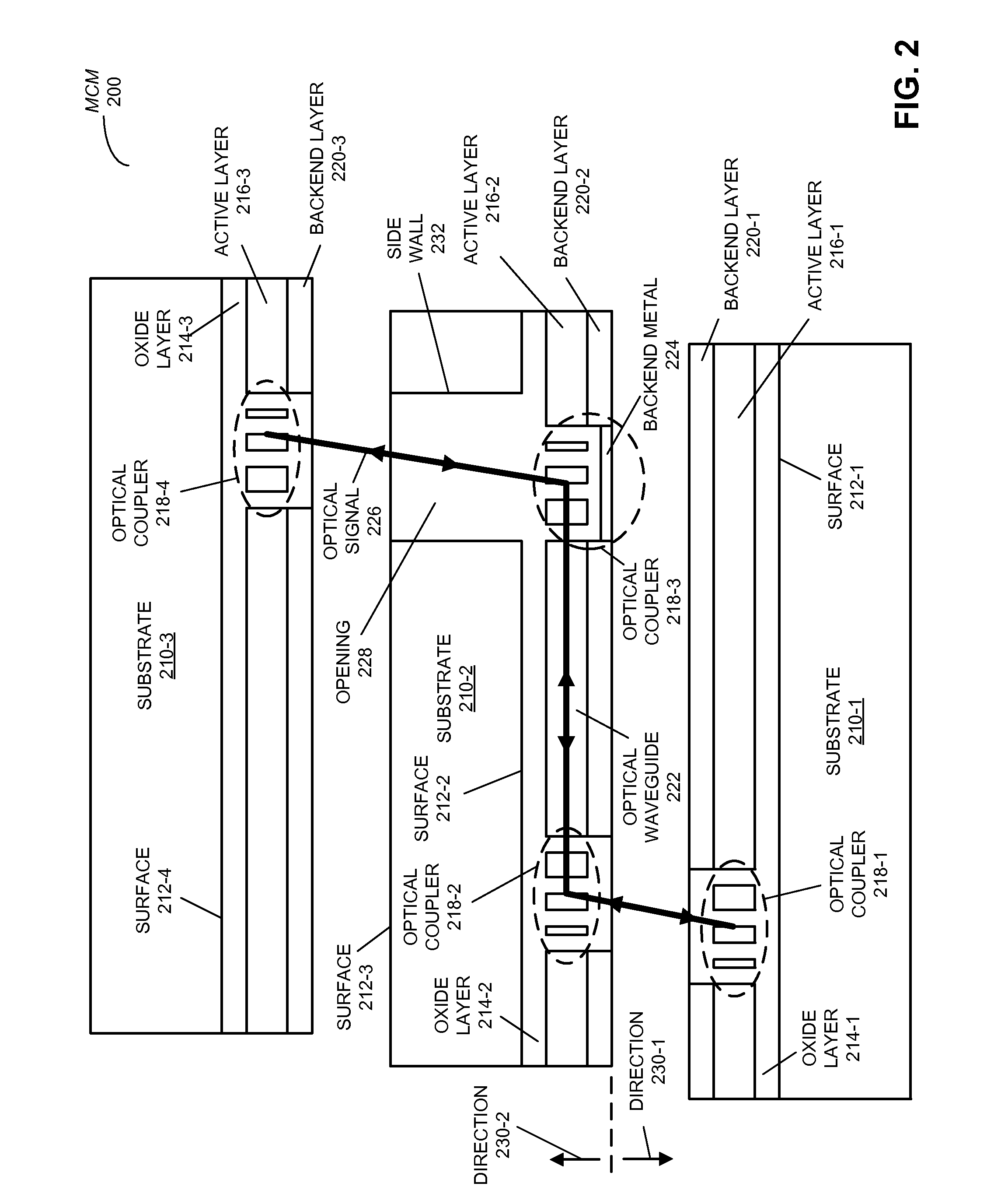
[0036]Embodiments of a multi-chip module (MCM), a system that includes the MCM, and a technique for coupling an optical signal using the MCM are described. This MCM includes a three-dimensional (3D) stack of chips that are coupled using optical interconnects. In particular, disposed on a first surface of a middle chip in the 3D stack there a...


PUM


Abstract

A multi-chip module (MCM), which includes a three-dimensional (3D) stack of chips that are coupled using optical interconnects, is described. In this MCM, disposed on a first surface of a middle chip in the 3D stack, there are: a first optical coupler, an optical waveguide, which is coupled to the first optical coupler, and a second optical coupler, which is coupled to the optical waveguide. The first optical coupler redirects an optical signal from the optical waveguide to a first direction (which is not in the plane of the first surface), or from the first direction to the optical waveguide. Moreover, the second optical coupler redirects the optical signal from the optical waveguide to a second direction (which is not in the plane of the first surface), or from the second direction to the optical waveguide. Note that an optical path associated with the second direction passes through an opening in a substrate in the middle chip.

Description

GOVERNMENT LICENSE RIGHTS[0001]The United States Government has a paid-up license in this invention and the right in limited circumstances to require the patent owner to license others on reasonable terms as provided for by the terms of Agreement No. HR0011-08-9-0001 awarded by the Defense Advanced Research Projects Administration.BACKGROUND[0002]1. Field[0003]The present disclosure relates to a multi-chip module (MCM) that accommodates semiconductor chips. More specifically, the present disclosure relates to an MCM that includes a vertical stack of semiconductor chips with inter-chip optical interconnects.[0004]2. Related Art[0005]Engineers have recently proposed using a multi-chip module (MCM) (which is sometimes referred to as a ‘macro-chip’) to integrate a collection of semi-conductor chips. This MCM offers unprecedented computational density, energy efficiency, bisection bandwidth and reduced message latencies. These characteristics are obtained by photonically interconnecting ...

Claims


Application Information

Patent Timeline
18 Sep 2012
Publication
US8267583B2
IPC
G02B6/26; G02B6/12; G02B6/34
CPC
G02B6/13; G02B6/12002
Inventors
YAO, JIN; ZHENG, XUEZHE