System and method for resource allocation of semiconductor testing industry

a technology for semiconductor testing and resource allocation, applied in the field of system and method for resource allocation in the semiconductor testing industry, can solve the problems of time-consuming planning and capacity allocation, conflict, delay and waste of resources, etc., and achieve the effect of efficient resource planning and capacity allocation

Inactive Publication Date: 2012-09-18
NAT TAIWAN UNIV OF SCI & TECH
View PDF23 Cites 1 Cited by
  • Summary
  • Abstract
  • Description
  • Claims
  • Application Information

AI Technical Summary

Benefits of technology

[0007]The present invention provides a system and a method for the semiconductor testing industry to efficiently develop resource planning and capacity allocation in a multiple resource environment.
[0011]In light of the above, based on the order information of customers and the production information of the on-hand resources, during multiple planning periods and under conditions of multiple resources and multiple orders, the present invention readily facilitates firms on decisions concerning resource planning, the product testing function requirements, resource allocation, and order acceptance under conditions of multiple planning periods, multiple resources, and multiple products so that corporate profit is maximized. The system for resource allocation uses the information obtained by the input module and uses the industry characteristic conversion module to convert the industry characteristic into the constraints. Subsequently, the artificial intelligence evolution module performs the evolution and in cooperation with an infeasible plan repairing module, solution searching is executed more efficiently.

Problems solved by technology

However, the orders to be tested and the required resource are complex combined resources (e.g., an order may simultaneously require a testing system, a handler and other machinery), which often lead to confliction, delay and waste among the resources.
Hence, if optimal resource planning and capacity allocation cannot be simultaneously achieved, thereby possibly leading to losses in millions of dollars.
A conventional method for resource planning and capacity allocation is time consuming, and many what-if analyses cannot be easily performed in a short time.
There is also a lack of methods to precisely describe operational characteristics in the semiconductor testing industry (e.g. factors such as fabrication feasibility between resources, production feasibility between orders and resources and constraints on production capacity of resources).

Method used


Image

  • System and method for resource allocation of semiconductor testing industry
  • System and method for resource allocation of semiconductor testing industry
  • System and method for resource allocation of semiconductor testing industry

Examples


Embodiment Construction

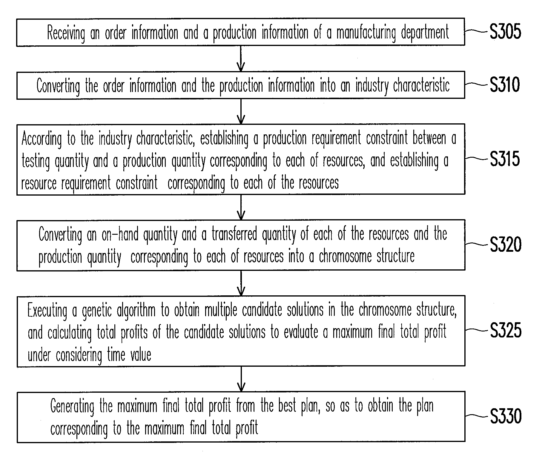
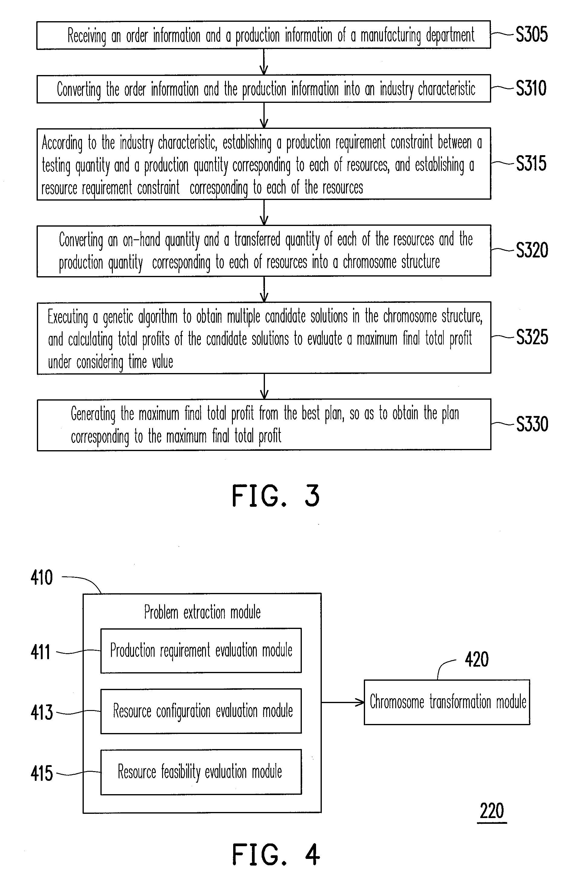
[0020]The semiconductor testing industry is a capital intensive industry. In order to effectively use costly resources of such industry (e.g. machinery equipment and human resources), the present invention provides a method and system for resource allocation in the semiconductor testing industry, so that obtainment of and configuration of the resources are well planned under multiple resource planning constraints. In order to make the present invention more comprehensible, embodiments are described below as the examples to prove that the present invention can be embodied.

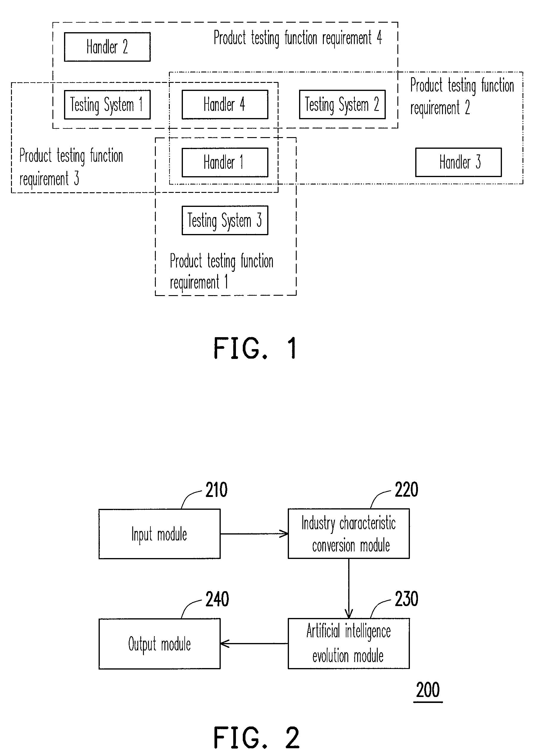
[0021]FIG. 1 is a schematic diagram showing a multiple resource environment in a semiconductor testing factory according to an embodiment of the present invention. Referring to FIG. 1, according to the present embodiment, the resources in the semiconductor testing factory include testing systems 1 to 3 and handlers 1 to 4. Here, product testing function requirements 1 to 4 are given by the customers. As shown in FIG...


PUM


Abstract

A system and a method for resource allocation in the semiconductor testing industry are provided. In the system, an industry characteristic conversion module is used to transform the industry characteristic obtained from an input module into a chromosome structure. Next, an artificial intelligence evolution module proceeds to find an optimal solution by handling the chromosome structure until a candidate solution having a maximum final total profit converges to a value.

Description

CROSS-REFERENCE TO RELATED APPLICATION[0001]This application claims the priority benefit of Taiwan application serial no. 98101787, filed on Jan. 17, 2009. The entirety of the above-mentioned patent application is hereby incorporated by reference herein and made a part of specification.BACKGROUND OF THE INVENTION[0002]1. Field of the Invention[0003]The present invention relates to a system and a method for planning and allocating resources in the semiconductor testing industry, and particularly to a system and a method for resource allocation in the semiconductor testing industry in a multiple resource environment.[0004]2. Description of Related Art[0005]Due to increasing competition between firms, based on market prediction, semiconductor testing firms must effectively perform resource planning, capacity allocation, profit allocation, and resource purchasing to allocate capacity to orders / semiconductor chips of customers, so that the profits and the resources can be employed most e...

Claims


Application Information

Patent Timeline
Patent Type & Authority Patents(United States)
IPC IPC(8): G06Q10/00
CPCG06Q10/06G06Q10/063Y02P90/80
Inventor WANG, KUNG-JENGWANG, SHIH-MIN
Owner NAT TAIWAN UNIV OF SCI & TECH
Why Eureka
Try Eureka