
Pulse signal delay circuit and LED drive circuit
a signal delay and led drive technology, applied in pulse manipulation, pulse technique, instruments, etc., can solve the problems of reducing the freedom of setting the frequency, unable to ignore the abnormal sounds described above, and unable to achieve the effect of preventing flickering and emission, preventing inconsistency in brightness, and preventing the effect of inconvenient operation
- Summary
- Abstract
- Description
- Claims
- Application Information
AI Technical Summary
Benefits of technology
Problems solved by technology
Method used
Image

Examples
first embodiment
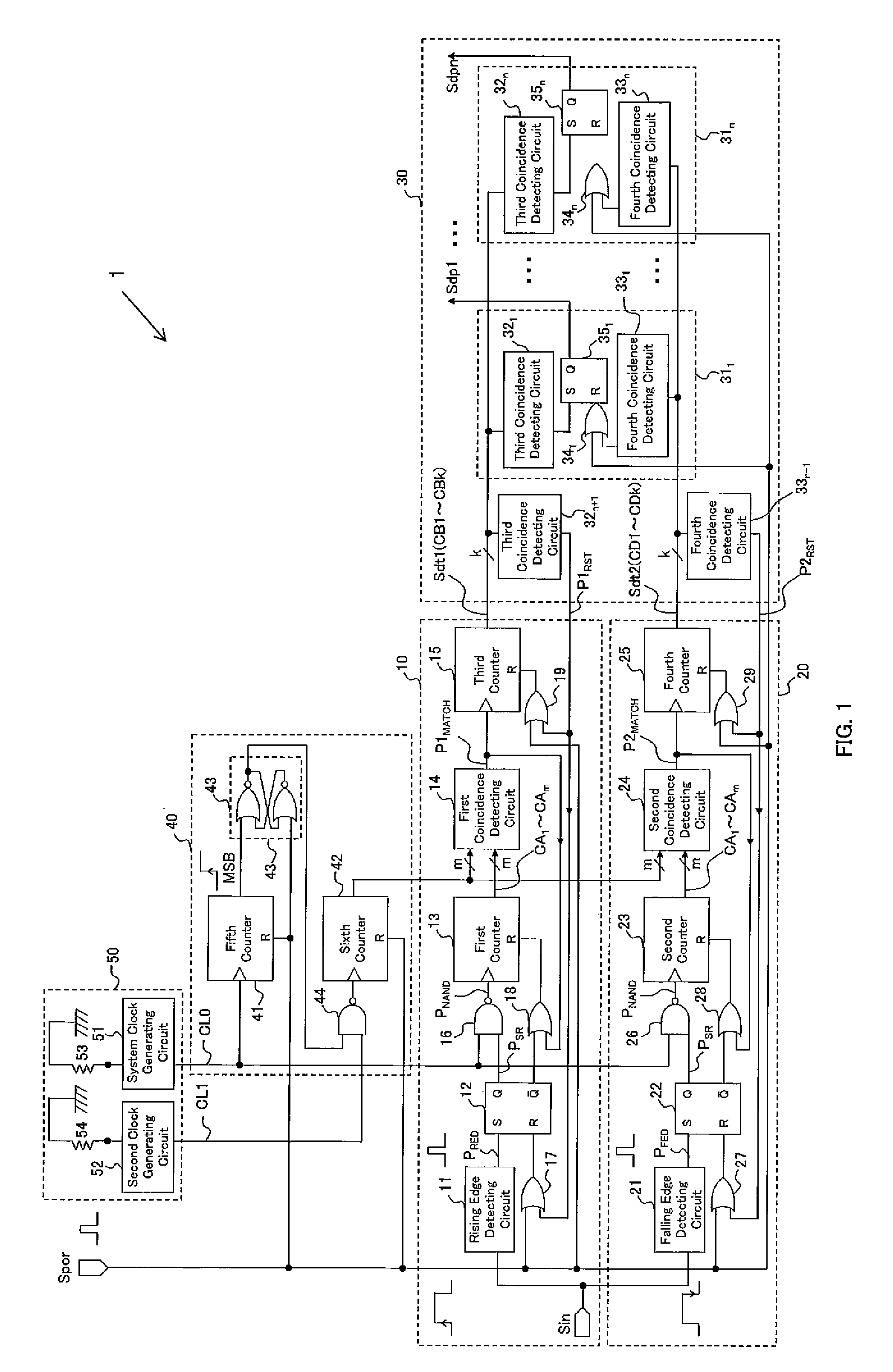
[0043]FIG. 1 is a logic circuit block diagram showing the circuit configuration of the pulse signal delay circuit according to the first embodiment of the present invention. The pulse signal delay circuit according to the present embodiment (hereinafter abbreviated to as “present delay circuit”) is formed of five circuit block sections. Concretely, as shown in FIG. 1, the present delay circuit 1 is configured by five circuit blocks: a first pulse edge delay circuit 10, a second pulse edge delay circuit 20, a delay pulse signal generating circuit 30, a delay counter value generating circuit 40 and a clock generating circuit 50.
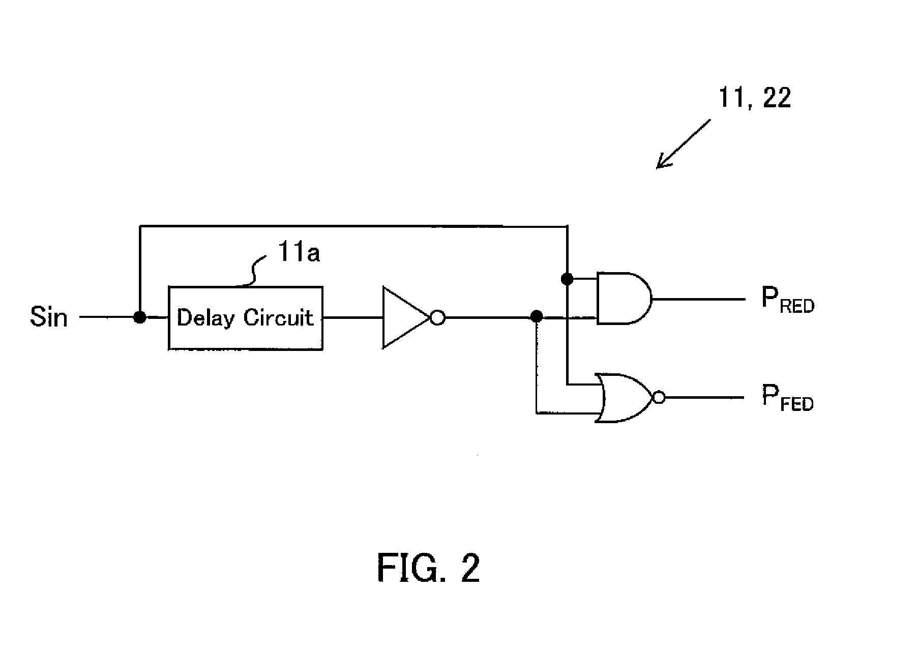
[0044]The first pulse edge delay circuit 10 detects a rising edge of the PWM signal Sin being an input pulse signal, and generates a first delay timing signal Sdt1 for sequentially outputting the first edge detection delay timing, gained by delaying the detection timing of the rising edge by a preset delay time Δt a predetermined number of times (n) within one ...
second embodiment
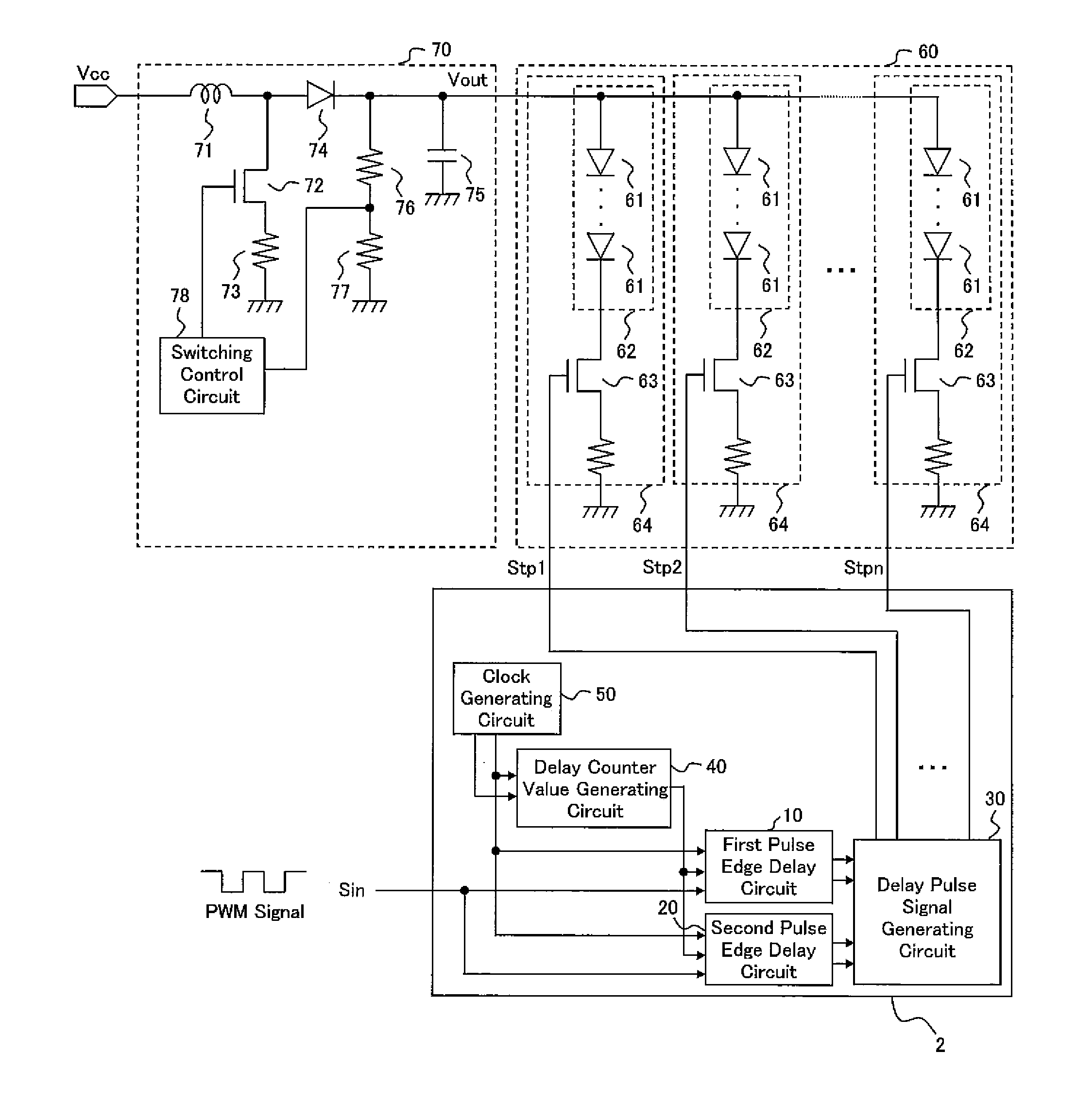
[0066]Next, the LED drive circuit according to one embodiment of the present invention is described. The LED drive circuit according to the present embodiment (hereinafter abbreviated to as “present drive circuit”) is configured using the present delay circuit 1 according to the first embodiment. Accordingly, this circuit configuration is the same as that of the present delay circuit 1 shown in FIG. 1 and is configured by five circuit blocks: a first pulse edge delay circuit 10, a second pulse edge delay circuit 20, a delay pulse signal generating circuit 30, a delay counter value generating circuit 40 and a clock generating circuit 50. As shown in FIG. 5, the present drive circuit 2 is an LED drive circuit for driving an LED circuit 60, which is configured by connecting in parallel a plurality (n) of circuit units 64 (641 to 64n) gained by connecting in series an LED series circuit 62 gained by connecting a plurality of LEDs 61 in series in the same direction and a drive transistor...
PUM
 Abstract
Description
Claims
Application Information