Load driving circuit and multi-load feedback circuit
a feedback circuit and load technology, applied in pulse technique, process and machine control, instruments, etc., can solve the problems of achieve the effect of improving efficiency, stable light emission, and lowering the efficiency of the led driving apparatus
- Summary
- Abstract
- Description
- Claims
- Application Information
AI Technical Summary
Benefits of technology
Problems solved by technology
Method used
Image
Examples
first embodiment
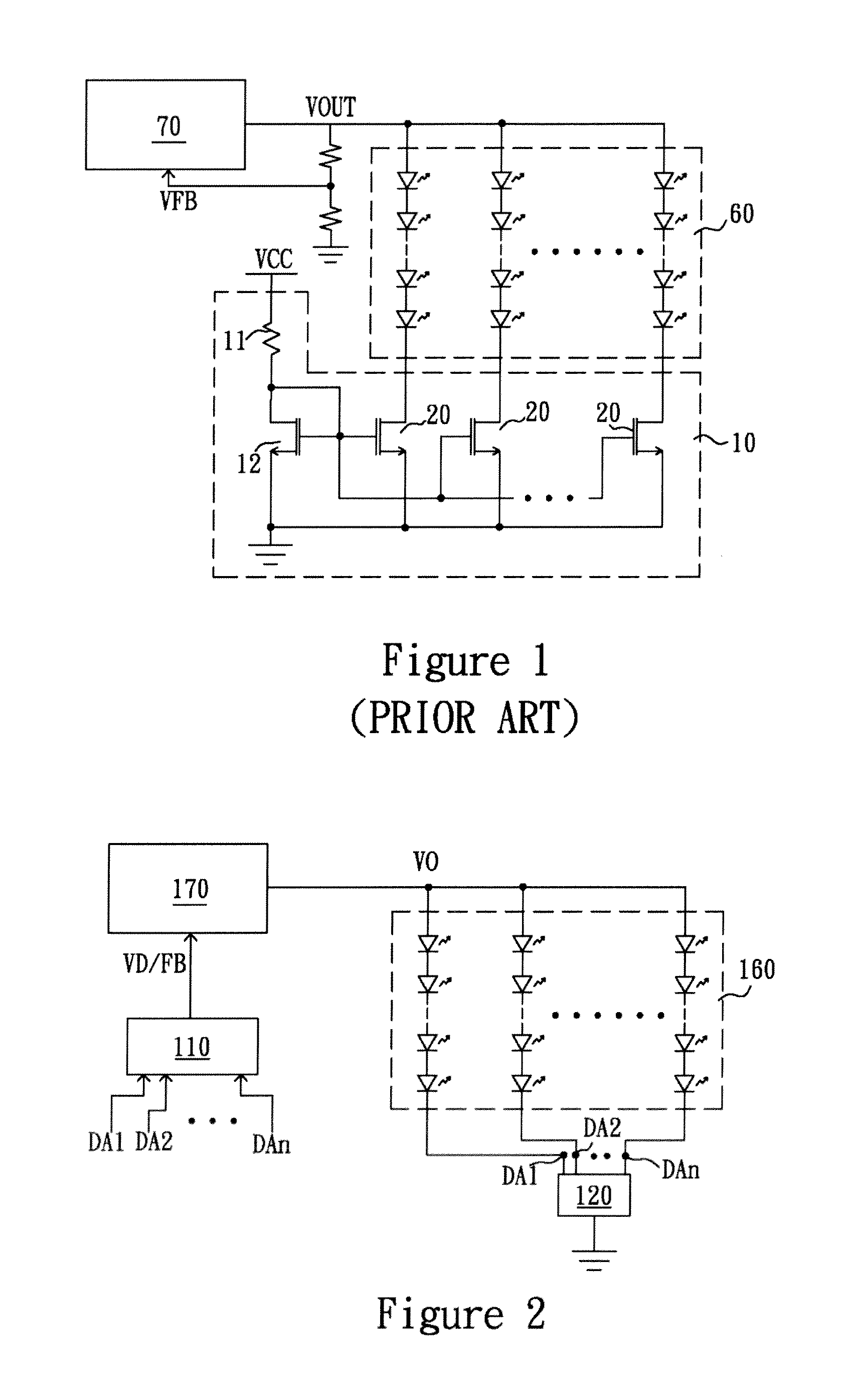
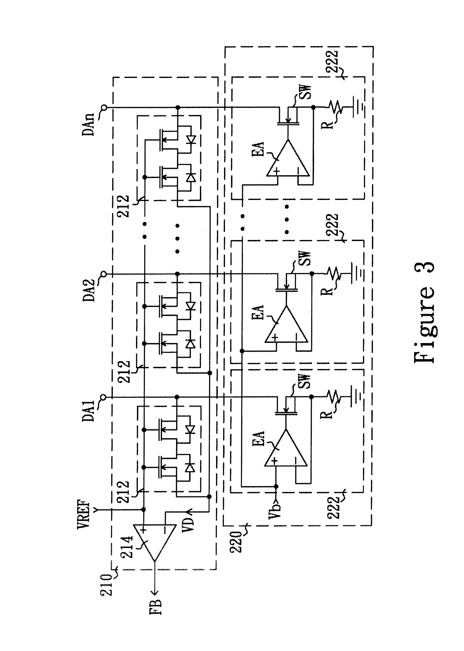
[0024]Next, refer to FIG. 3, wherein a schematic diagram of the multi-load feedback circuit according to the present invention is shown. The present multi-load feedback circuit 210 comprises a plurality of semiconductor switches 212 and a determining circuit 214. Each semiconductor switch has a first terminal, a second terminal and a third terminal. The first terminals are coupled to a common reference voltage VREF. The second terminals are individually coupled to the plurality of current balancing terminals DA1˜DAn of the current balancing circuit 220; that is, coupled to the plural LED strings in the LED module 160. The third terminals are coupled with each other and also coupled to the determining circuit 214, thereby generating a detection signal VD to the determining circuit 214.
[0025]The current balancing circuit 220 includes a plurality of current balancing units 222, with each current balancing unit 222 including a transistor switch SW, a resistor R and an error amplifier EA...
second embodiment
[0029]Refer next to FIG. 4, wherein a schematic diagram of the multi-load feedback circuit according to the present invention is shown. The multi-load feedback circuit 310 comprises a plurality of semiconductor switches 312, an error amplifier 314, a resistor 316 and a transistor switch 318. Each semiconductor switch 312 has a first terminal, a second terminal and a third terminal. The first terminals are coupled to a common reference voltage VREF. The second terminals are individually coupled to the plurality of current balancing terminals DA1˜DAn of the current balancing circuit 320. The third terminals are coupled with each other and also coupled to the error amplifier 314 thereby generating a detection signal VD to the error amplifier 314. In the present embodiment, the circuits and operations of the semiconductor switch 312 is identical to which of the semiconductor switch 212 illustrated in FIG. 3, descriptions thereof are thus omitted for brevity.
[0030]The most significant di...
third embodiment
[0031]Subsequently, refer to FIG. 5, wherein a schematic diagram of the multi-load feedback circuit according to the present invention is shown. Compared with the multi-load feedback circuit 212 depicted in FIG. 3, each gate of the MOSFETs', having the sources thereof coupled to the current balancing terminals DA1˜DAn, is coupled to the corresponding current balancing terminal, rather than the common reference voltage VREF, so the MOSFET is maintained in a cutoff state. When the level at the current balancing terminal is lower than the common reference voltage VREF by a predetermined voltage difference thereby causing the corresponding multi-load feedback circuit 412 to be in a conducting state, the signal of the current balancing terminal will be passed to the inverse terminal of the comparator 414 through the body diode of the MOSFET in cutoff and another MOSFET conducted. As a result, the multi-load feedback circuit 412 according to the present embodiment can, as the multi-load f...
PUM
 Abstract
Description
Claims
Application Information


