SRAM writing system and related apparatus

a writing system and random access memory technology, applied in static storage, information storage, digital storage, etc., can solve the problem that it is much more difficult for pass-gate transistors to meet the conflicting requirements of data read and write, and achieve the effect of improving the driving ability, speeding up the recovery of normal write bit-lines, and enhancing the conduction of pre-charge circuits

Active Publication Date: 2012-12-04
FARADAY TECH CORP
View PDF3 Cites 10 Cited by
  • Summary
  • Abstract
  • Description
  • Claims
  • Application Information

AI Technical Summary

Benefits of technology

[0007]On the other hand, for writing data to a cell, the corresponding pair of bit-lines are respectively charged and discharged to high level and low level respectively; when the pass-gate transistors are turned on, the pair of bit-lines will respectively charge / discharge the two data nodes through respective pass-gate transistors. Therefore, turn-on resistance of pass-gate transistors is preferably to be lower such that level of the data nodes can be rapidly charged / discharged to level of the bit-lines.
[0020]One dummy replica cell of the dummy replica bit-line is used as a indication cell; this dummy replica cell stores a dummy data according to level of the dummy replica write bit-line, so the write ending controller can correspondingly generate a write ending signal according to data in the dummy replica cell; according to level transition of the write ending signal, the word-line timing signal and the write control signal can transit level to end the write cycle. That is, when each normal writing circuit starts to write data to the normal cell under the control of the write control signal, the dummy replica writing circuit also writes the dummy data to the indication cell through the dummy replica write bit-line under the control of the write control signal. As initial data of the indication cell is changed to the dummy data by writing, writing completion of the dummy replica write bit-line is indicated, and writing of the normal write bit-lines can be ended correspondingly: the write ending controller will reflect ending in the write ending signal, so the write cycle of the memory can be ended as soon as possible. In this way, period for writing can be effectively shortened to reduce memory operation cycle and increase memory operation frequency (rate).

Problems solved by technology

As advanced semiconductor process evolves and demand on low operation voltage emerges, it becomes much more difficult for pass-gate transistors to fulfill conflicting requirements of data read and write.

Method used


Image

  • SRAM writing system and related apparatus
  • SRAM writing system and related apparatus
  • SRAM writing system and related apparatus

Examples


Embodiment Construction

[0031]It is to be understood that other embodiment may be utilized and structural changes may be made without departing from the scope of the present invention. Also, it is to be understood that the phraseology and terminology used herein are for the purpose of description and should not be regarded as limiting. The use of “including,”“comprising,” or “having” and variations thereof herein is meant to encompass the items listed thereafter and equivalents thereof as well as additional items. Unless limited otherwise, the terms “connected,”“coupled,” and “mounted,” and variations thereof herein are used broadly and encompass direct and indirect connections, couplings, and mountings.

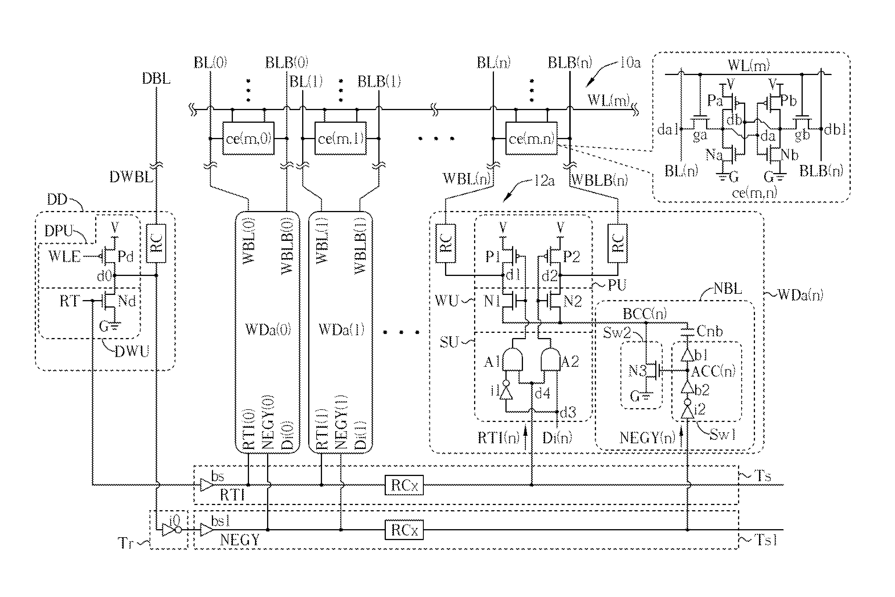
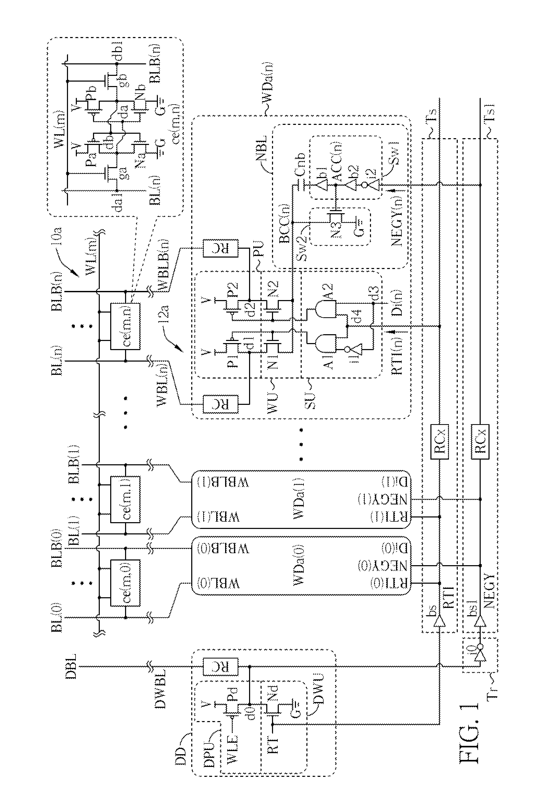
[0032]Please refer to FIG. 1 illustrating a circuit of a memory 10a according to an embodiment of the invention. In this embodiment, the memory 10a can be an SRAM with a plurality of cells aligned in matrix; cells of the m-th row which are commonly coupled to the word-line WL(m) include cells ce(m,0) of the...


PUM


Abstract

SRAM writing system and related apparatus are provided. The writing system of the invention has a dummy replica writing circuit, a negative pulse controller and at least a normal writing circuit; each normal writing circuit includes a write driver and a negative pulse supplier. While writing, the dummy replica writing circuit drives a dummy replica bit-line, such that the negative pulse controller generates a negative pulse control signal according to level of the dummy replica bit-line. In each writing circuit, when the write driver conducts to connect an associated bit-line to a bias end for driving a level transition, the negative pulse supplier switches the bias end from an operation voltage to a different negative pulse voltage according to the received negative pulse control signal.

Description

[0001]This application claims the benefit of Taiwan application Serial No. 99108935, filed Mar. 25, 2010, the subject matter of which is incorporated herein by reference.FIELD OF THE INVENTION[0002]The present invention relates to SRAM (Static Random Access Memory) writing system and related apparatus, and more particularly, to SRAM writing system and related apparatus controlling timing of introducing negative pulse voltage according to level transition of a dummy replica write bit-line for improving writing accuracy and speed of SRAM, speeding up bit-line recovery, shortening SRAM operation cycle, and raising SRAM operation frequency.BACKGROUND OF THE INVENTION[0003]Semiconductor memory, such as SRAM, is an essential building block of modern electronic systems. Generally, a memory has a plurality of cells aligned in matrix; cells of a same row are coupled to a same word-line, and cells of a same column are coupled to a same bit-line (or a same pair / group of bit-lines). For accessi...

Claims


Application Information

Patent Timeline
Patent Type & Authority Patents(United States)
IPC IPC(8): G11C11/00
CPCG11C11/413
Inventor CHUANG, CHING-TESHIH, WEI-CHIANGLEE, HUNG-YULIN, JIHI-YUTU, MING-HSIENJOU, SHYH-JYELEE, KUN-DI
Owner FARADAY TECH CORP
Why Eureka
Try Eureka