PCB with soldering pad projections forming fillet solder joints and method of production thereof

a technology of printed circuit board and soldering pad, which is applied in the manufacture of final products, sustainable manufacturing/processing, and the incorporation of printed electric components. it can solve the problems of low yield of electronic devices, failure of soldering, and difficulty in forming side electrodes at the outer edges of electronic devices. it can prevent the failure of bonding, and prevent the failure of electronic devices. the effect of yield drop

Active Publication Date: 2012-12-25
FUJITSU LTD
View PDF21 Cites 7 Cited by
  • Summary
  • Abstract
  • Description
  • Claims
  • Application Information

AI Technical Summary

Benefits of technology

[0012]An object of the present invention is to provide a printed circuit board and / or a method of production of an electronic apparatus for carrying an electronic device having device bottom electrodes by soldering on a printed circuit board so as to prevent bonding failure between the electronic device and the printed circuit board.
[0017]According to the present invention, a projection is provided at a board electrode, so the molten solder remains between the electrodes, the height of the molten solder between the electrodes is raised, and that molten solder absorbs warping of the electronic device and printed circuit board at the time of reflow, so it is possible to prevent bonding failure between an electronic device having device bottom electrodes and a printed circuit board and possible to prevent a drop in yield of the electronic apparatuses surface mounting electronic devices having device bottom electrodes.
[0018]Furthermore, according to the present invention, it is possible to prevent bonding failure of device bottom electrodes, which occupy a smaller area on a printed circuit board than device side electrodes, at a printed circuit board and thereby provide a higher density electronic apparatus.

Problems solved by technology

However, if the solder melted by the reflow does not stop at between the electronic device electrodes and the board electrodes and leaks outside of the electronic device, sometimes the warping of the electronic device and the printed circuit board at the time of reflow will result in soldering failure etc. and the problem of a drop in yield of the electronic apparatuses.
It is therefore difficult to form side electrodes at the outer edges of an electronic device.
The board electrodes are extended in the direction of the outer edges of the electronic device and the area occupied by the electronic device on the printed circuit board is increased, so there is the problem that this impairs the increased density of electronic apparatuses.

Method used


Image

  • PCB with soldering pad projections forming fillet solder joints and method of production thereof
  • PCB with soldering pad projections forming fillet solder joints and method of production thereof
  • PCB with soldering pad projections forming fillet solder joints and method of production thereof

Examples


Embodiment Construction

[0024]Below, embodiments of the present invention will be explained with reference to the drawings.

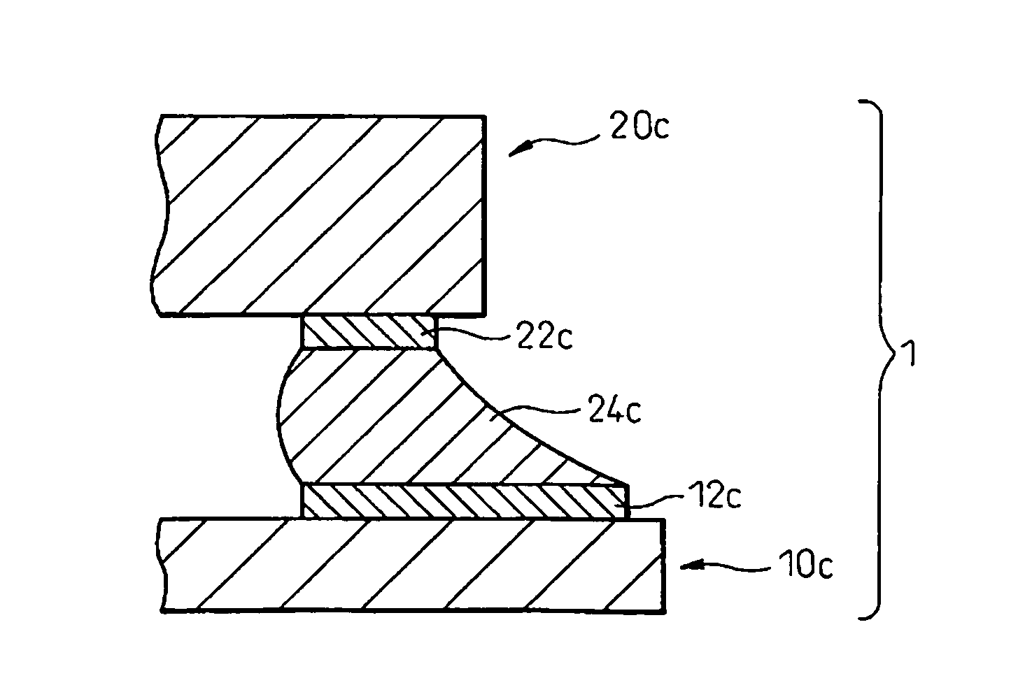
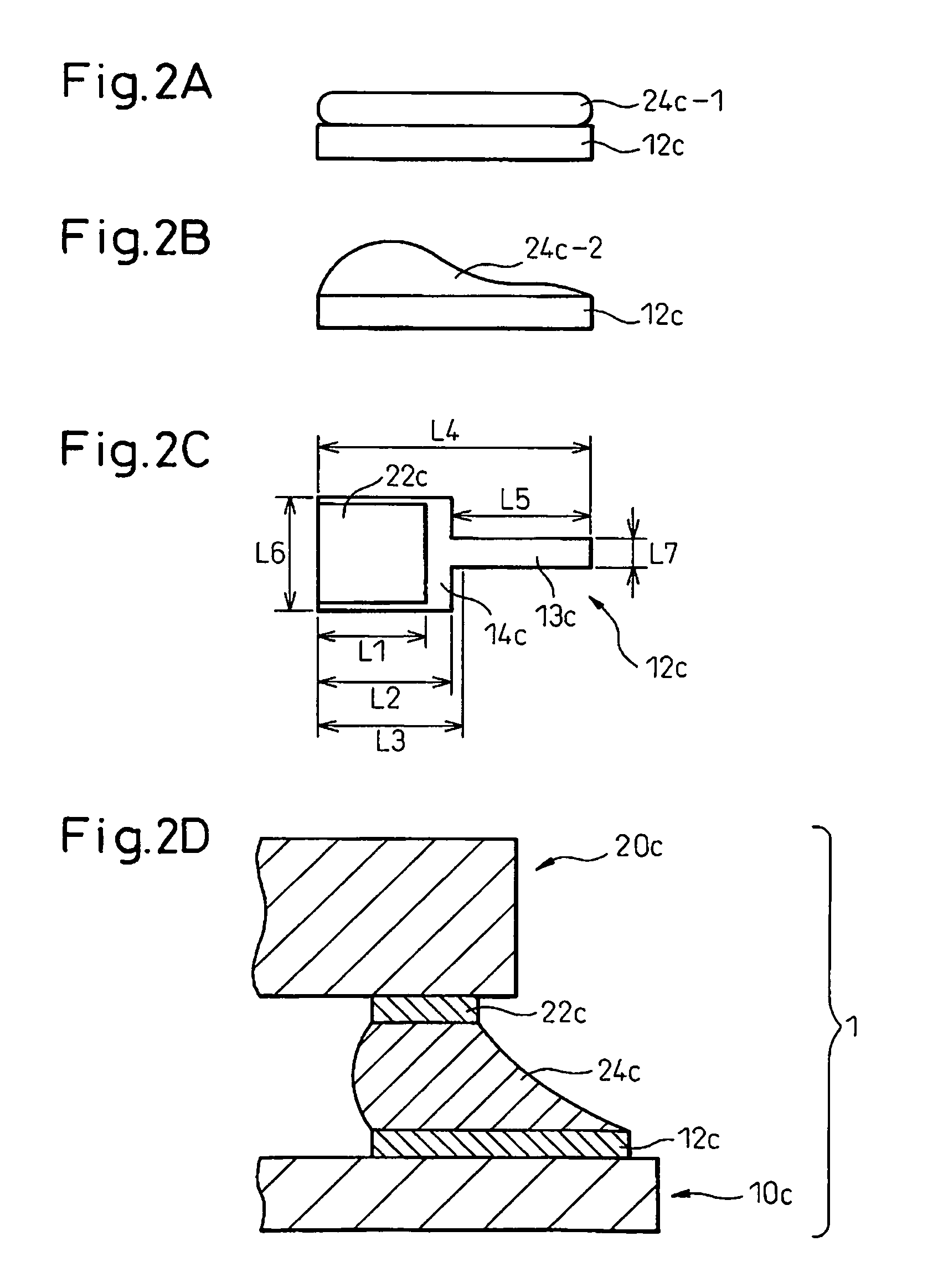
[0025]Using FIGS. 2A to 2D, in an electronic apparatus, an example of a board electrode provided on a printed circuit board, a device bottom electrode provided on an electronic device, and a solder joint will be explained.

[0026]FIG. 2A is a side view showing the state before reflow where a board electrode 12c is coated with a solder paste, FIG. 2B is a side view showing the shape of the solder paste, coated on the board electrode 12c, at the time of reflow, FIG. 2C is a top view showing the positional relationship between a device bottom electrode 22c and a board electrode 12c having a board electrode base 14c and a projection 13c, and FIG. 2D is a side view showing the state where a device bottom electrode 22c of an electronic device 20c and a board electrode 12c of the printed circuit board 10c are bonded through a solder joint 24c in an electronic apparatus 1.

[0027]The board electro...


PUM

PropertyMeasurementUnit
widthaaaaaaaaaa
surface tensionaaaaaaaaaa
electrical testaaaaaaaaaa

Abstract

A printed circuit board provided with board electrodes, wherein each board electrode is provided with a board electrode base, for carrying by soldering a bottom electrode arranged at a bottom of an electronic device inside from outer edges of the electronic device, arranged inside from the outer edges of the electronic device and a projection projecting out from the board electrode base, narrower in width than the board electrode base, and connected to an interconnect of the printed circuit board.

Description

BACKGROUND OF THE INVENTION[0001]1. Field of the Invention[0002]The present invention relates to a printed circuit board and a method of production of an electronic apparatus.[0003]2. Description of the Related Art[0004]In the past, integrated circuits, resistors, capacitors, and numerous other electronic devices have been surface mounted on printed circuit boards by reflow soldering.[0005]Normally, for surface mounting an electronic device on a printed circuit board by reflow soldering, first a printing plate for printing solder paste is arranged over the board electrodes of the printed circuit board and cream-like solder paste is coated on the printing plate to coat the board electrodes with solder paste. Next, the printing plate is removed, the electronic device is placed on the printed circuit board, and solder melted by hot air heating or infrared heating called “reflow” is used to bond the electronic device electrodes and the board electrodes.[0006]A printed circuit board carr...

Claims


Application Information

Patent Timeline
Patent Type & Authority Patents(United States)
IPC IPC(8): H05K1/03H05K1/16
CPCH05K1/111H05K3/3442H05K3/3484Y10T29/4913H05K2201/10636H05K2201/10727H05K2203/0545H05K2201/09381H01L2224/16105H01L24/16H01L24/81H01L2224/16058H01L2224/16238H01L2924/3841H05K3/3485Y02P70/50H05K1/02H05K1/09H05K1/03
Inventor HIRANO, YOSHIKAZUABE, MITSUNORI
Owner FUJITSU LTD
Why Eureka
Try Eureka