Metal/ceramic bonding article and method for producing same

a technology of metal/ceramic bonding and metal/ceramic, which is applied in the manufacture of cables/conductors, metallic pattern materials, solid-state devices, etc., can solve the problems of resistor easy to occur, bonding failure, and deterioration of productivity, so as to reduce the displacement failure of parts and improve productivity.

Inactive Publication Date: 2005-02-22
DOWA METALS & MINING CO LTD
View PDF17 Cites 4 Cited by
  • Summary
  • Abstract
  • Description
  • Claims
  • Application Information

AI Technical Summary

Benefits of technology

It is therefore an object of the present invention to eliminate the aforementioned problems and to provide a metal/ceramic bond

Problems solved by technology

In particular, when a very small resistor having a size of 10 mm□, such as a hunt resistive element, is bonded to a ceramic substrate, the displacement of the resistor is easy to occur, and it is difficult to bond one or a plurality of resistors to one ceramic substrate, so that there is a problem in that the displacement fai

Method used


Image

  • Metal/ceramic bonding article and method for producing same
  • Metal/ceramic bonding article and method for producing same
  • Metal/ceramic bonding article and method for producing same

Examples


example 1

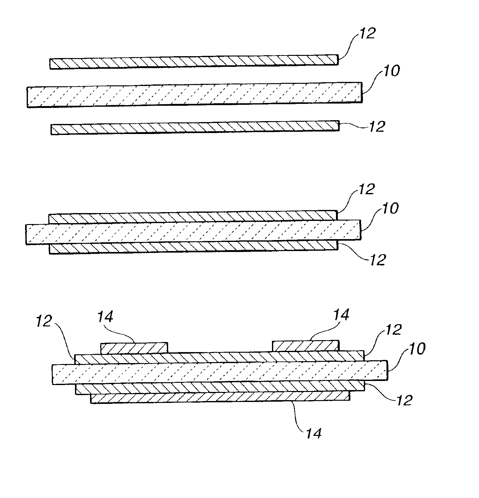
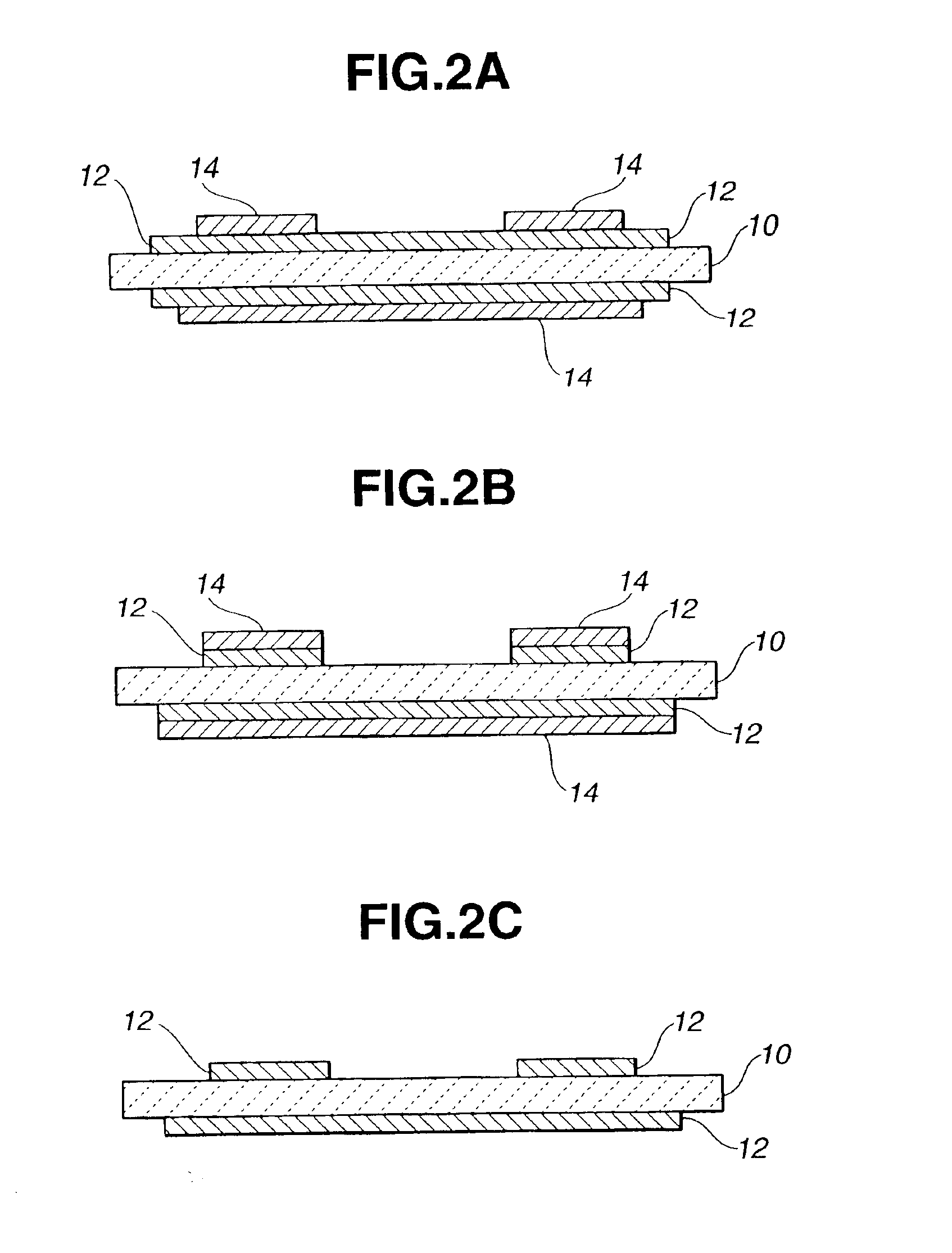
Plates of a Cu—Ni—Mn alloy (manganin) having a size of 56×75 mm□ and a thickness of 0.2 mm and serving as a resistive alloy were arranged directly on both sides of an alumina substrate having a size of 60×80 mm□ and a thickness of 0.635 mm to be heated in an atmosphere of nitrogen to a maximum temperature of 975° C. to obtain a metal / ceramic bonding article. Then, resists having a size of 48×68 mm□ (MT-UV-5203 produced by Mitsui Chemical Co., Ltd.) were printed on the manganin plates, and the manganin plates were etched with a copper chloride solution to remove undesired portions of the manganin plates. Then, the resists were removed.

With respect to ten substrates thus obtained, the displacement fraction defective was measured on the basis of ±0.2 mm as a criterion, so that the displacement fraction defective was 0%.

example 2

An alumina substrate having a size of 60×80 mm□ and a thickness of 0.635 mm was prepared, and a break line processing was carried out so as to separate the alumina substrate into 35 regions, each having a size of 10×10 mm□, while ensuring a dummy portion of 5 mm in the edge portion thereof. Thereafter, plates of a Cu—Ni—Mn alloy (manganin) having a size of 56×75 mm□ and a thickness of 0.2 mm and serving as a resistive alloy were arranged directly on both sides of the alumina substrate to be heated in an atmosphere of nitrogen to a maximum temperature of 975° C. to obtain a metal / ceramic bonding article. Then, 35 resists, each having a size of 8×8 mm□ (MT-UV-5203 produced by Mitsui Chemical Co., Ltd.), were printed on the manganin plates so that each of the resists corresponds to the center of each of the 35 regions of 10×10 mm□ on the alumina substrate, and the manganin plates were etched with a copper chloride solution to remove undesired portions of the manganin plates. Then, the ...

example 3

With respect to the metal / ceramic bonding article obtained by the same method as that in Example 2, the same etching process as that in Example 2 was carried out, and the resists were removed. Thereafter, the substrate thus obtained was dipped in a 10% solution of Enplate PC455 (Meltex Co., Ltd.) at 47° C. for 325 seconds to be degreased, and dipped in a solution of CPB50+35% H2O2 water (47%+4%) (Mitsubishi Gas Chemical Co., Inc.) at 45° C. for 70 seconds to be chemical-polished. Then, the substrate was dipped in sulfuric acid (10%) at room temperature for 30 seconds to be acid-pickled, and dipped in a 10% solution of Melplate Activator 350 (Meltex Co., Ltd.) at 30° C. for 220 seconds to carry out a catalyst application. Thereafter, the substrate was dipped in a solution of Nimuden SX-M+SX-A (10%+5.5%) (C. Uyemura & Co., Ltd.) at 84° C. for 8 minutes to carry out the electroless Ni—P plating on the entire surface of the manganin plates.

After the substrate thus obtained was divided i...


PUM

PropertyMeasurementUnit
Temperatureaaaaaaaaaa
Electrical resistanceaaaaaaaaaa
Shapeaaaaaaaaaa

Abstract

There is provided a method for producing a metal/ceramic bonding article, the method including the steps of: bonding a metal plate 12 of an alloy containing copper and nickel directly to at least one side of a ceramic substrate 10; applying a resist 14 on a predetermined portion of the metal plate 12 to remove an undesired portion of the metal plate 12 by etching; and removing the resist 14 to form a pattern having a predetermined shape of the alloy on the ceramic substrate 10. According to this method, it is possible to reduce the displacement failure of parts to improve productivity and to prevent bonding failure during the mounting of a semiconductor device or the like thereon.

Description

BACKGROUND OF THE INVENTION1. Field of the InventionThe present invention generally relates to a metal / ceramic bonding article having a ceramic substrate and a metal plate bonded to the ceramic substrate, and a method for producing the same. More specifically, the invention relates to a metal / ceramic bonding article wherein a metal plate of a Cu—Ni or Cu—Mn—Ni alloy serving as a resistive element is bonded to a ceramic substrate and which is used for an electronic member for resistance, such as a shunt resistive element, and a method for producing the same.2. Description of the Prior ArtIn conventional electronic members for resistance, such as shunt resistive elements, an alloy plate serving as a sheet resistor precisely worked by a press working or the like is bonded to a ceramic substrate via a brazing filler metal, such as an Ag brazing filler, by means of the brazing and soldering (see Japanese Patent Laid-Open No. 11-97203).However, in such an electronic member bonded via a br...

Claims


Application Information

Patent Timeline
IPC IPC(8): C04B37/02H05K1/16H05K1/09H05K1/03C04B37/00H01L23/12H01L23/14
CPCB32B18/00C04B37/021H05K1/09H05K1/167Y10T428/24917B32B2311/12B32B2311/22C04B2235/96C04B2237/343C04B2237/40C04B2237/405C04B2237/407C04B2237/408C04B2237/704C04B2237/706H05K1/0306H05K2201/0355C04B2235/656C04B2235/658C04B2237/32Y10T428/12882Y10T29/49155Y10T428/24926Y10T29/49156Y10T428/12861Y10T428/12944Y10T428/12611Y10T29/49128Y10T428/12535B32B2311/04
Inventor TSUKAGUCHI, NOBUYOSHITAKAHASHI, TAKAYUKIKITAMURA, YUKIHIROKIMURA, MASAMI
Owner DOWA METALS & MINING CO LTD
Why Eureka
Try Eureka