Data-aware dynamic supply random access memory

a random access memory and data-aware technology, applied in the field of random access memory, can solve the problems of weak strength disadvantageous to write, data read and data write mutual conflict, etc., and achieve the effects of reducing read disturb, improving read static noise margin (rsnm), and reducing read confli

Active Publication Date: 2013-01-01
FARADAY TECH CORP +1
View PDF6 Cites 12 Cited by
  • Summary
  • Abstract
  • Description
  • Claims
  • Application Information

AI Technical Summary

Benefits of technology

[0005]Cell access operation of RAM is described as follows. While Reading data of a data storage node in a cell, a bit-line corresponding to the data node is first pre-charged to high voltage of logic 1. When Reading starts, the data storage node of the cell is connected to the bit-line by a corresponding pass-gate transistor; if the data storage node stores logic 0 of low voltage, the inverter in the cell pulls down the voltage of the bit-line to reflect stored data of logic 0. Before Reading starts, an n-channel MOS transistor in the inverter pulls down and hold the data storage node to low voltage so the data storage node can store logic 0. As Reading starts, however, voltage at the data storage node will be raised because the data storage node is connected to the bit-line which is at high voltage. Equivalently, the pass-gate transistor and the n-channel MOS transistor in the inverter form a voltage divider between high bit-line voltage of logic 1 and low voltage of logic 0 as Reading starts. If voltage at the data storage node is raised too high, it will exceed a trip voltage of the opposite inverter in the latch structure, and data of the data storage node will be incorrectly flipped from logic 0 to logic 1 by feedback mechanism of the latch structure. To prevent incorrect data flip during Read, weak pass-gate transistors (with narrower width or longer channels, lower conduction and larger source-drain resistance) are adopted in cells; whereas relatively strong (lower source-drain resistance) n-channel MOS transistors are used, such that the voltage at the data storage node will be contained to below the trip voltage of the opposite inverter to improve noise margin during Read.
[0007]In other words, requirements for data Read and data Write are mutually conflicting; and the conflict is more severe for compact layout / low operation voltage RAM / cell in advanced / scaled process. To mitigate the conflict of Read and Write operation, a RAM, with column-based independent supply controls for the two respective inverters in each cell of a column according to data voltages of bit-lines, is disclosed. In the disclosure of the invention, weak pass-gate transistors can be adopted to reduce Read disturb and improve Read Static Noise Margin (RSNM). To improve Write-ability and Write performance, when logic 0 is written to a data storage node originally storing logic 1, assuming the data storage node is held at high voltage (logic 1) by a p-channel MOS transistor of a first inverter, then, during Write operation, the power supply control of invention will reduce the source supply voltage of the p-channel MOS transistor of the first inverter, but maintain the source supply voltage of the p-channel MOS transistor of the opposite (second) inverter in the cell. Reducing source supply voltage of the p-channel MOS transistor of the first inverter lowers the Source-to-Gate voltage of the p-channel MOS transistor, thus reducing the conduction of the p-channel MOS transistor, so the pass-gate transistor between the data storage node and the bit-line can pull-down the data storage node to logic 0 much easier. Meanwhile, as source supply voltage for the p-channel MOS transistor of the opposite (second) inverter is maintained, the conduction of the p-channel MOS transistor of the opposite (second) inverter remains unchanged, thus the p-channel MOS transistor of the second inverter can rapidly pull-up the opposite data storage node to high voltage of logic 1. As aforementioned concept is implemented, bit-line voltages, i.e., data to be written, are used to determine whether source supply voltage reduction is applied to the p-channel MOS transistor of the first inverter or that of the second inverter.
[0008]Symmetrically, following aforementioned discussion, voltage supply to source of the n-channel MOS transistor of the first inverter can be raised to reduce voltage difference between its Gate and Source, so conduction of the n-channel MOS transistor is decreased to improve writing of logic 1 to the data storage node originally storing logic 0; meanwhile, source voltage supply of the n-channel MOS transistor of the opposite (second) inverter is maintained, so its conduction remains unchanged to rapidly pull-down the opposite data storage node to low voltage of logic 0.

Problems solved by technology

If weak pass-gate transistors are adopted to improve the Read noise margin, their weak strength would be disadvantageous for Write.
Again, if weak pass-gate transistors are adopted to improve Read noise margin, their weak strength would be disadvantageous for Write.
In other words, requirements for data Read and data Write are mutually conflicting; and the conflict is more severe for compact layout / low operation voltage RAM / cell in advanced / scaled process.

Method used


Image

  • Data-aware dynamic supply random access memory
  • Data-aware dynamic supply random access memory
  • Data-aware dynamic supply random access memory

Examples


Embodiment Construction

[0019]The present invention will now be described more specifically with reference to the following embodiments. It is to be noted that the following descriptions of preferred embodiments of this invention are presented herein for purpose of illustration and description only. It is not intended to be exhaustive or to be limited to the precise form disclosed.

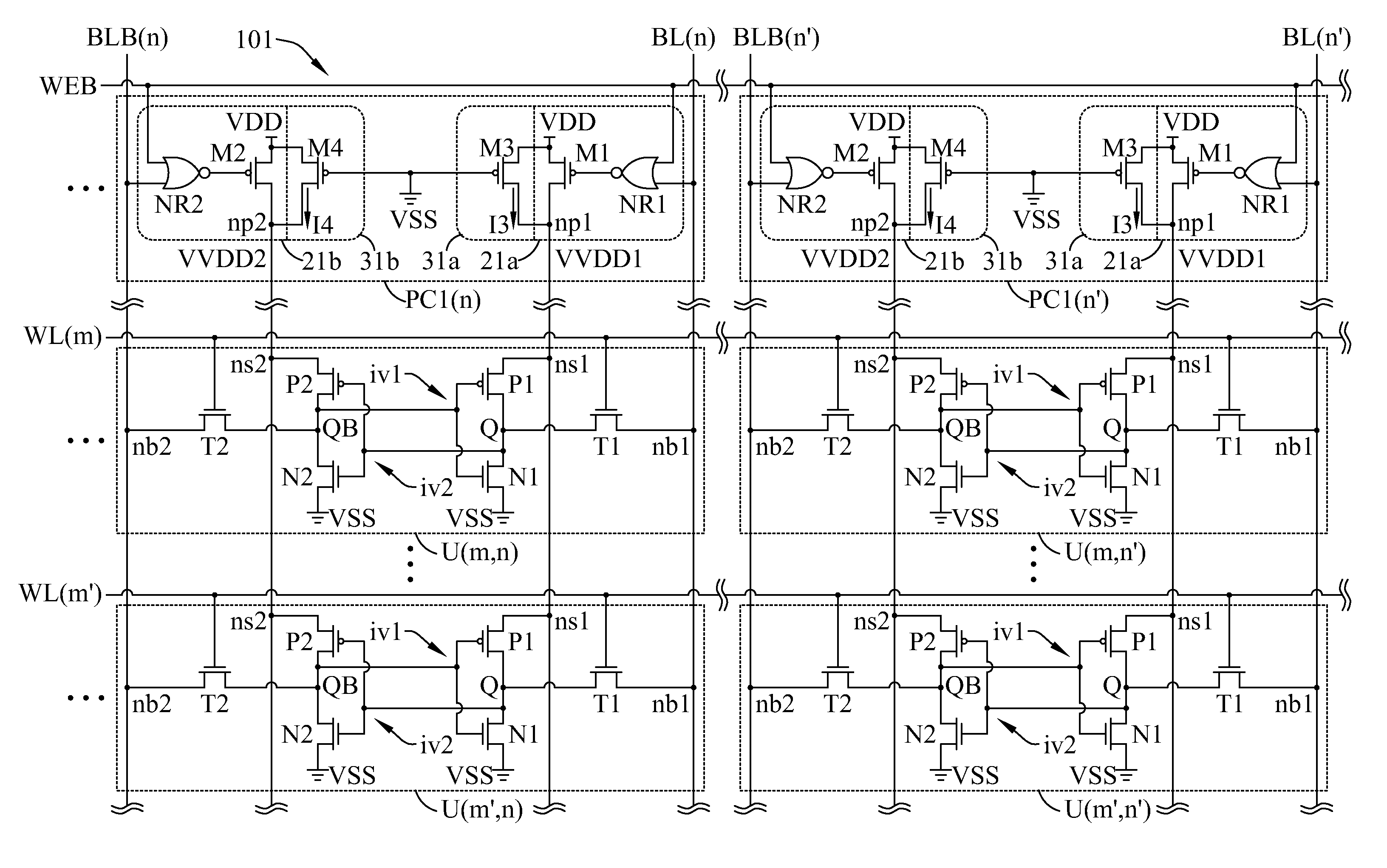
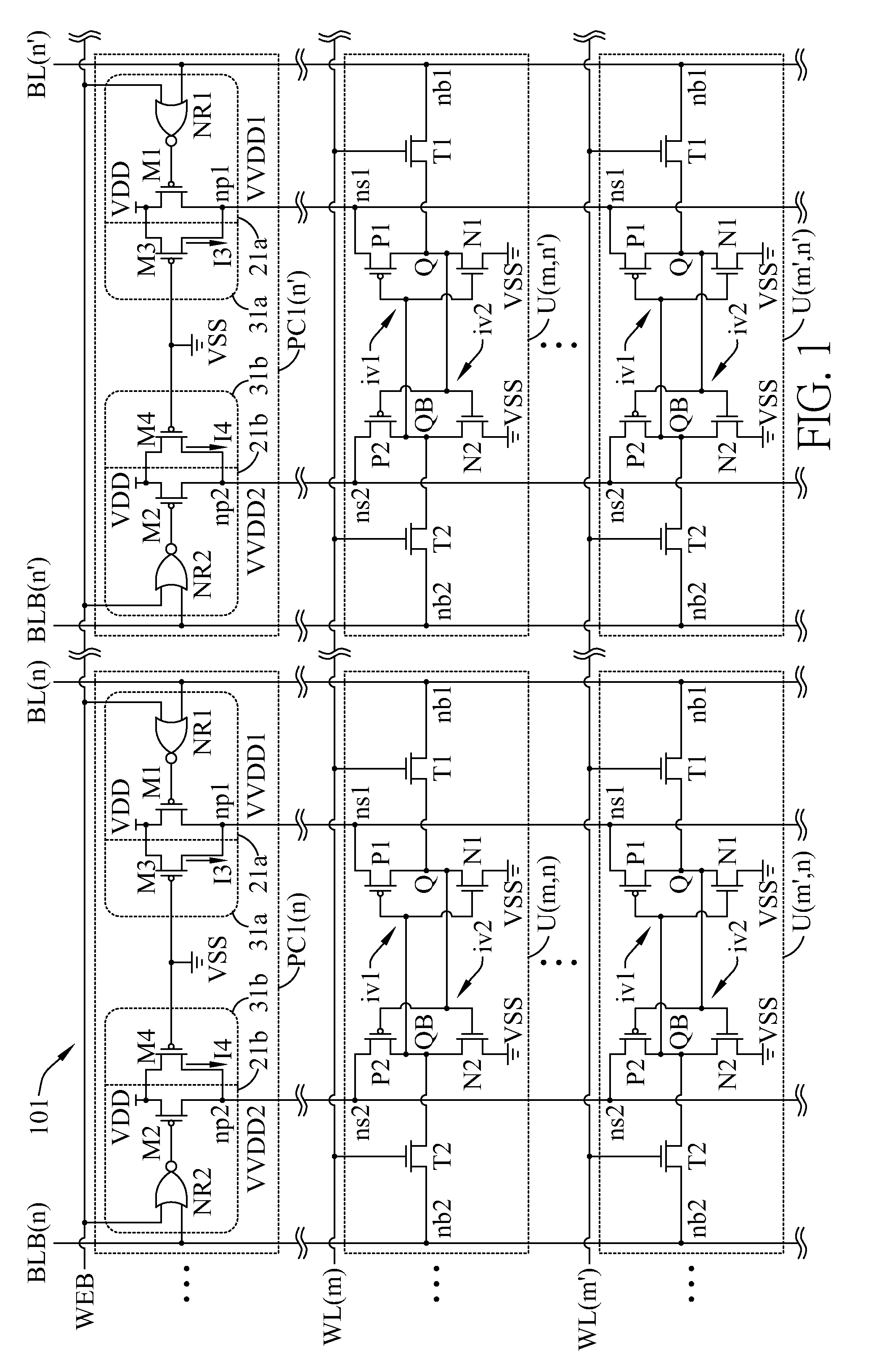
[0020]Please refer to FIG. 1 which illustrates a RAM 101 according to an embodiment of the invention. The RAM 101 can be a static RAM which includes a plurality of cells, such as cells U(m,n)U(m,n′)U(m′,n) and U(m′,n′) in FIG. 1; each cell is a 6T static RAM cell. These cells are arranged in an array of rows and columns; for example, the cells U(m,n) and U(m,n′) are arranged in a same row and correspond to a same word-line WL(m); the cells U(m′,n) and U(m′,n′) are arranged in another row and correspond to another word-line WL(m′). The cells U(m,n) and U(m′,n) are arranged in a same column and correspond to a pair of bit-lines BL(...


PUM


Abstract

A Random Access Memory (RAM) with a plurality of cells is provided. In an embodiment, the cells of a same column are coupled to a same pair of bit-lines and are associated to a same power controller. Each cell has two inverters; the power controller has two power-switches. For the cells of the same column, the two power-switches respectively perform independent supply voltage controls for the two inverters in each cell according to data-in voltages of the bit-lines during Write operation.

Description

[0001]This application claims the benefit of Taiwan application Serial No. 099127792, filed Aug. 19, 2010, the subject matter of which is incorporated herein by reference.FIELD OF THE INVENTION[0002]The present invention relates to a Random Access Memory (RAM), and more particularly, to a RAM with column-based independent supply controls for two respective inverters in each of Static RAM (SRAM) cells of a column to resolve the conflicting requirements of Read and Write operationsBACKGROUND OF THE INVENTION[0003]Random access memories, such as static RAM, have become one of the most important construction blocks of modern electronic systems. Modern RAM development demands small cell layout area and low operation voltage for improvement of density and power dissipation.SUMMARY OF THE INVENTION[0004]A RAM has a plurality cells arranged in an array of multiple columns and rows, each cell stores a bit of data for access. For example, a basic 6-Transistor (6T) static cell includes two inv...

Claims


Application Information

Patent Timeline
Patent Type & Authority Patents(United States)
IPC IPC(8): G11C11/40
CPCG11C11/413G11C11/412
Inventor CHUANG, CHING-TEYANG, HAO-ILIN, YI-WEIHWANG, WEISHIH, WEI-CHIANGCHEN, CHIA-CHENG
Owner FARADAY TECH CORP
Why Eureka
Try Eureka