

Semiconductor structure and a method of forming the same
a technology of semiconductors and iii-v materials, applied in the field of semiconductor structures, can solve the problems of low-quality gan layers, low-quality iii-v material layers that may comprise a large number of defects, and are not suitable for semiconductor devices
- Summary
- Abstract
- Description
- Claims
- Application Information
AI Technical Summary
Benefits of technology
Problems solved by technology
Method used
Image

Examples
Embodiment Construction
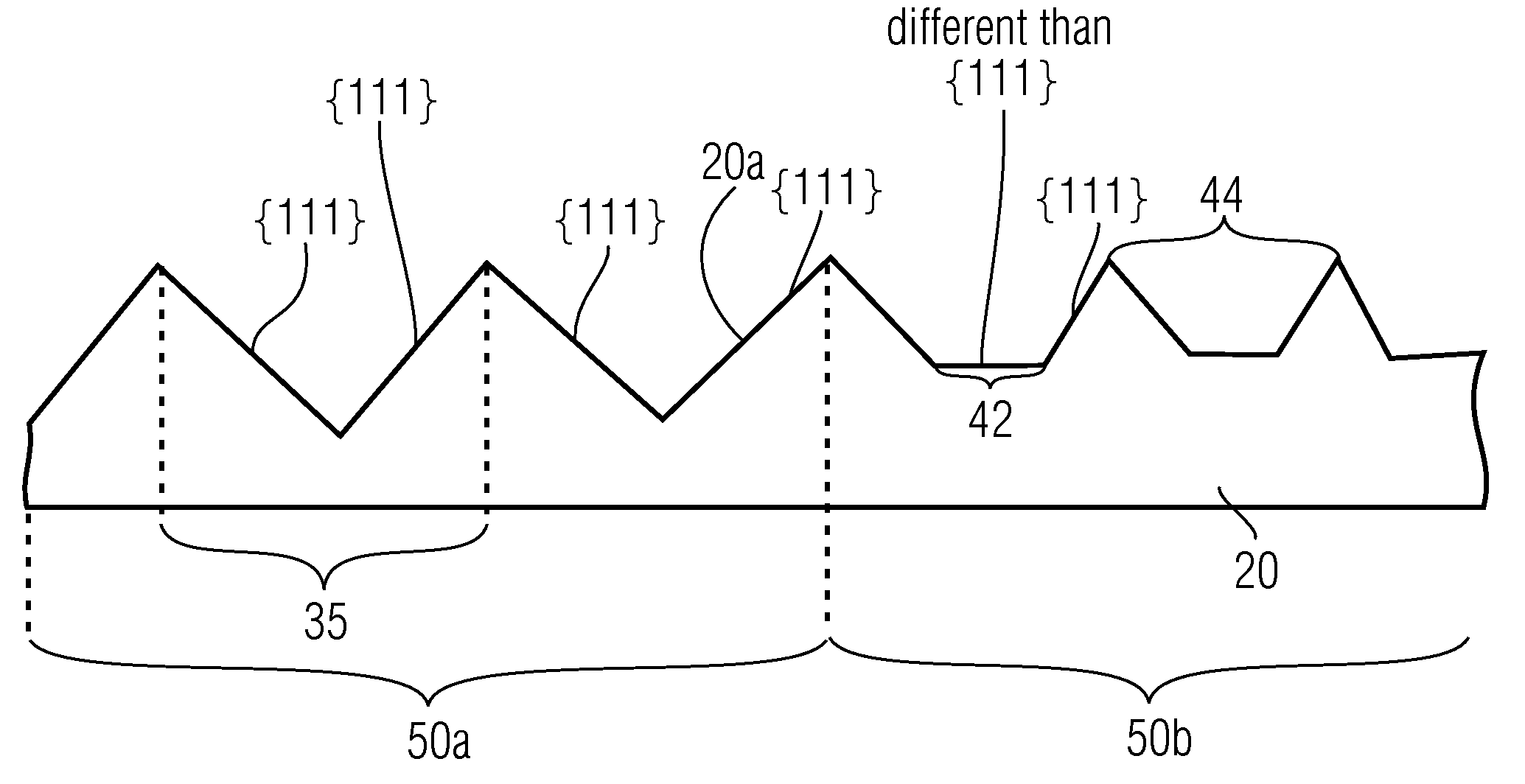
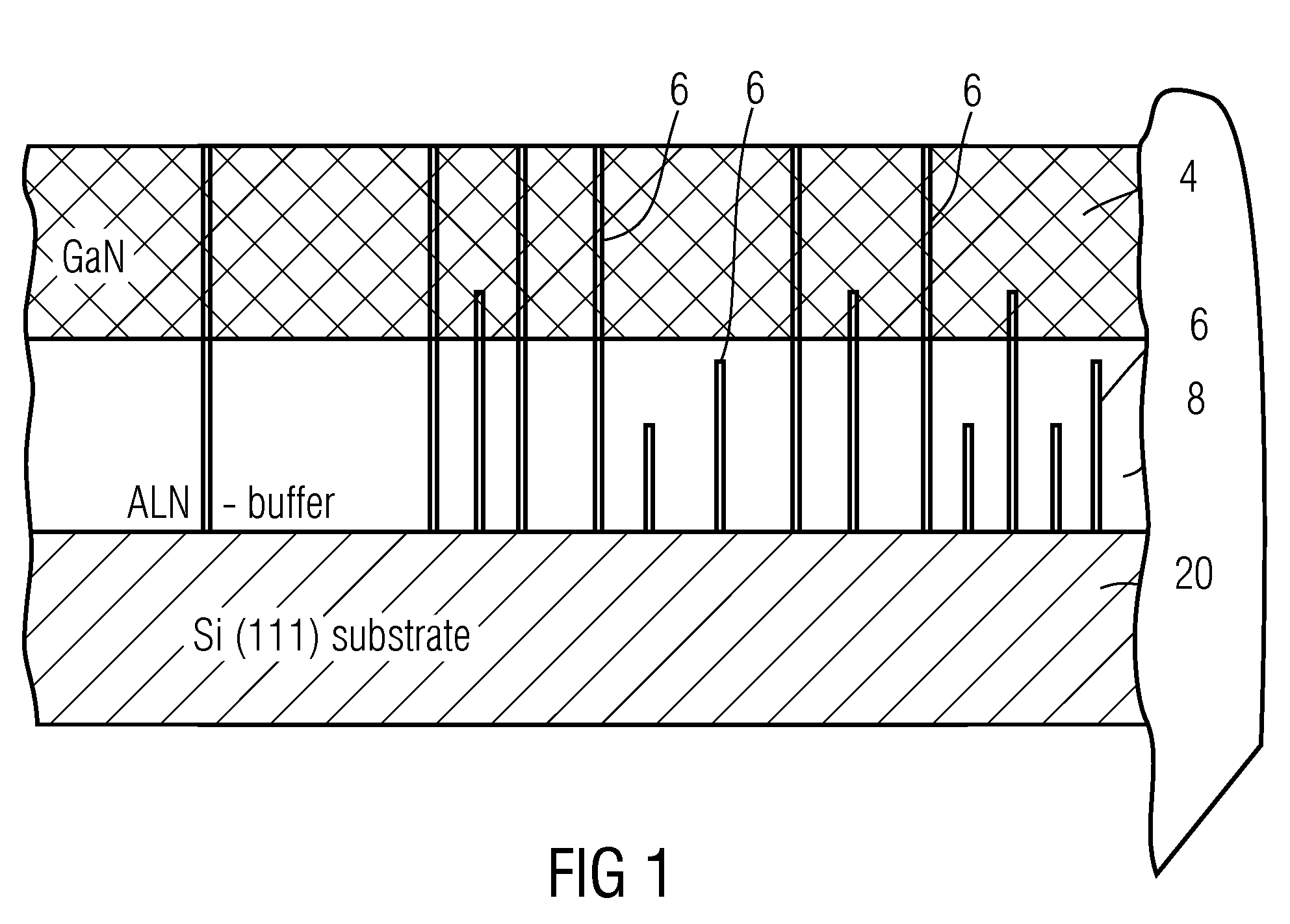
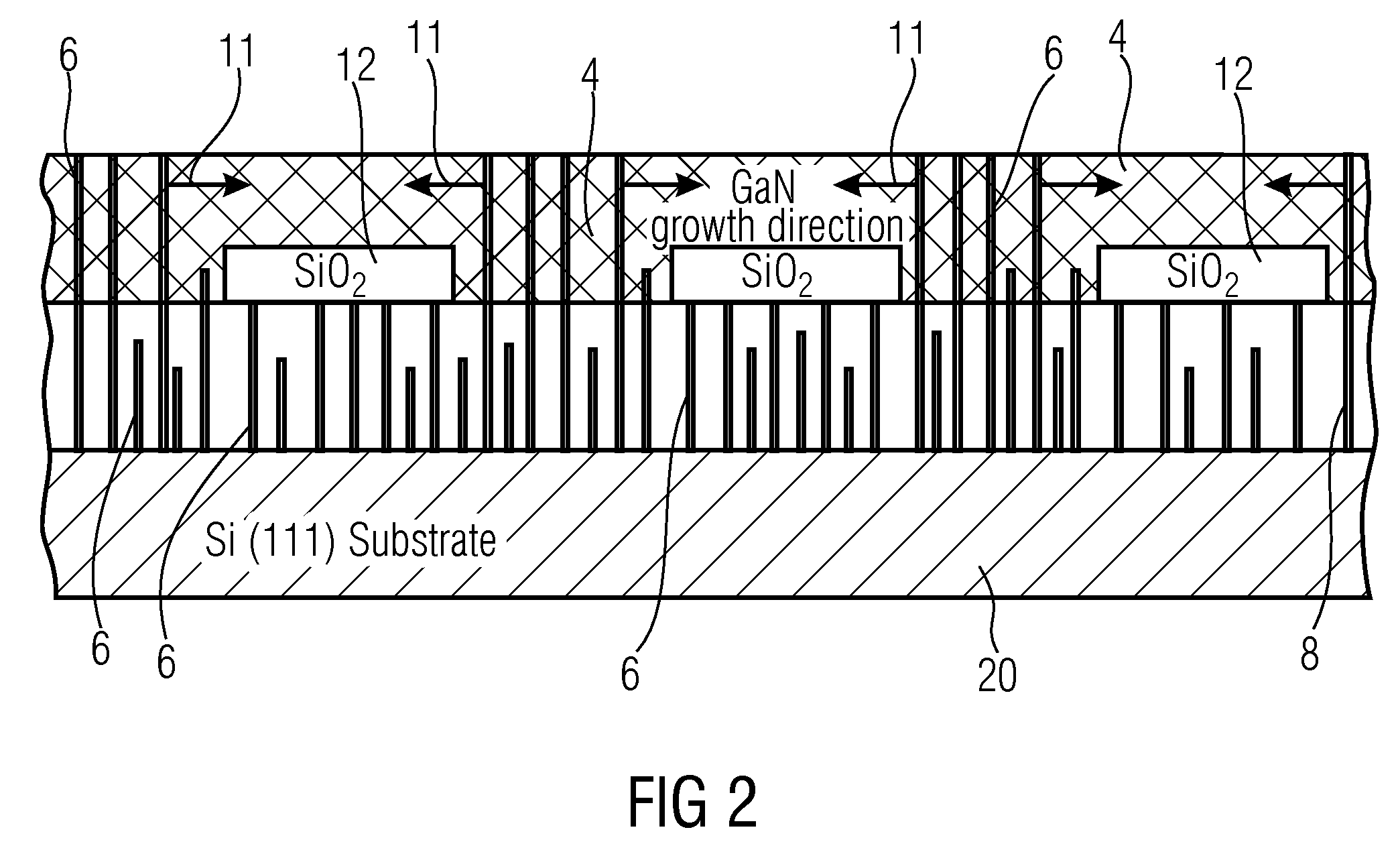
[0030]In FIG. 1, a schematic cross sectional view of a semiconductor structure is shown. The semiconductor structure comprises a silicon substrate 20, an aluminum nitride (AlN) buffer layer 8 and a gallium nitride (GaN) layer 4. The gallium nitride layer 4 comprises a plurality of dislocation defects or slip lines 6. The slip lines 6 typically develop in efforts to epitaxially grow a crystal material on a substrate of a different kind of material. These slip lines 6 may emerge from the substrate 20 during the growth of crystalline nitride, e.g., the AlN buffer layer 8, on the substrate 20. The crystal lattice of the substrate 20 may be different to the crystal lattice of the epitaxial grown III-V material layer 4, e.g., gallium nitride. Due to the crystal lattice mismatch, this means that due to the different crystalline lattice size of the two material types a mechanical stress, tensions or crystal lattice compression strength in the epitaxial grown III-V material layer 4 may occur...
PUM
 Abstract
Description
Claims
Application Information