Supercharge Your Innovation With Domain-Expert AI Agents!

Retardation substrate, method of manufacturing the same, and liquid crystal display

a technology of retardation substrate and liquid crystal display, which is applied in the field of optical techniques, can solve the problems of difficult to adopt optimal designs into all the pixels, retardation film may not compensate for the retardation of liquid crystal cells, and the problem is often more serious. achieve the effect of easy manufacturing of a retardation layer

Inactive Publication Date: 2013-01-08
TOPPAN PRINTING CO LTD
View PDF7 Cites 0 Cited by
  • Summary
  • Abstract
  • Description
  • Claims
  • Application Information

AI Technical Summary

Benefits of technology

The technical effect of this patent is to make it easy to make a retardation layer that has regions that cause different retardations.

Problems solved by technology

For this reason, it is difficult to adopt optimal designs into all the pixels different in display color.
For this reason, when employing a design for sufficiently compensating the retardation of a liquid crystal cell using a retardation film at pixels that display a certain color, the retardation film may insufficiently compensate the retardation of a liquid crystal cell at pixels that display other colors.
In fact, since the birefringence is greater on the short-wavelength's side of the visible range, i.e., within the blue wavelength range and is smaller on the long-wavelength's side of the visible range, i.e., within the red wavelength range, this problem is often more serious.
For this reason, when the above-described techniques are employed, the design for the color filter layer is limited or the degree of difficulty in manufacturing the color filter layer increases.

Method used


Image

  • Retardation substrate, method of manufacturing the same, and liquid crystal display
  • Retardation substrate, method of manufacturing the same, and liquid crystal display
  • Retardation substrate, method of manufacturing the same, and liquid crystal display

Examples


Embodiment Construction

[0028]An embodiment of the present invention will be described below with reference to the accompanying drawings. Note that the same reference symbols in the drawings denote components that achieve the same or similar functions, and a repetitive explanation thereof will be omitted.

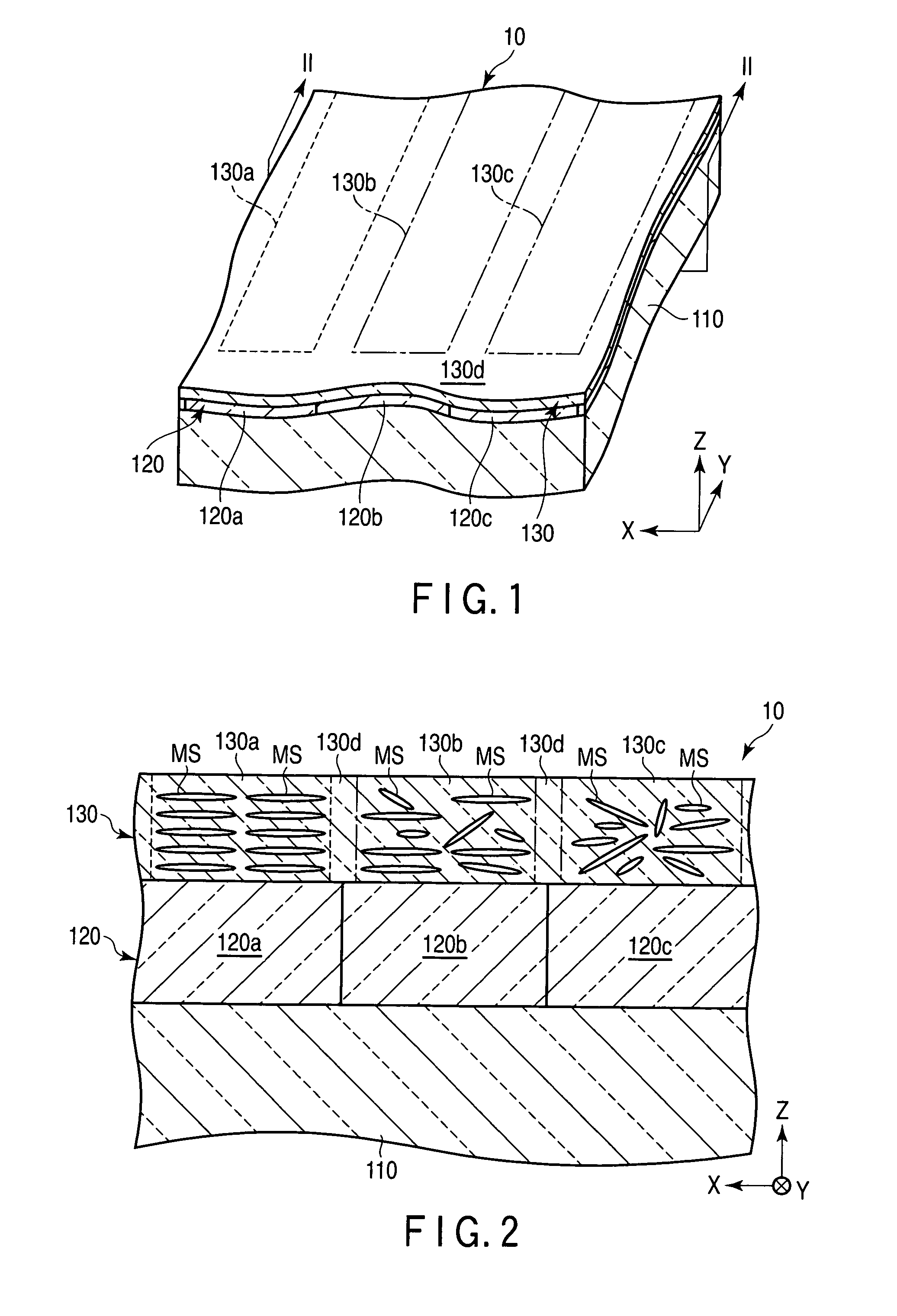
[0029]FIG. 1 is a perspective view schematically showing a retardation substrate according to an embodiment of the present invention. FIG. 2 is a sectional view taken along the line II-II of the retardation substrate shown in FIG. 1.

[0030]The retardation substrate 10 shown in FIGS. 1 and 2 includes a substrate 110, a color filter layer 120 and a solidified liquid crystal layer 130.

[0031]The substrate 110 has a light-transmitting property. The substrate 110 is, for example, a transparent substrate.

[0032]The color filter layer 120 is formed on the substrate 110. The color filter layer 120 includes coloring layers 120a to 120c different in absorption spectrum from one another and adjacent to one another on th...


PUM

PropertyMeasurementUnit
hazeaaaaaaaaaa
temperatureaaaaaaaaaa

Abstract

A retardation layer that includes regions causing different retardations can be manufactured easily. A retardation substrate includes a substrate and a solidified liquid crystal layer facing its main surface. The solidified liquid crystal layer includes first to third regions, and a degree of depolarization for each of the regions is less than 5.0×10⁻⁴. A difference between the maximum and minimum values of the degrees of depolarization obtained for the regions is less than 2.0×10⁻⁴.

Description

CROSS REFERENCE TO RELATED APPLICATIONS[0001]This is a Continuation Application of PCT Application No. PCT / JP2009 / 063365, filed Jul. 27, 2009, which was published under PCT Article 21(2) in Japanese.[0002]This application is based upon and claims the benefit of priority from prior Japanese Patent Application No. 2008-209250, filed Aug. 15, 2008, the entire contents of which are incorporated herein by reference.BACKGROUND OF THE INVENTION[0003]1. Field of the Invention[0004]The present invention relates to an optical technique that can be applied, for example, to a display such as liquid crystal display.[0005]2. Description of the Related Art[0006]Liquid crystal displays have characteristics of thin-shaped, lightweight and low power consumption. Thus, in recent years, their application to mobile devices and stationary equipments such as television receivers increases rapidly.[0007]In order to make it possible for a liquid crystal display to display a multi-colored image, a color filt...

Claims


Application Information

Patent Timeline
Patent Type & Authority Patents(United States)
IPC IPC(8): G02F1/1335
CPCG02B5/201G02B5/3016G02F1/13363G02F2413/09G02F2001/133633G02F1/133633G02F1/133631G02F1/1335G02B5/30
Inventor AKAO, SOSUKEKUBO, YUJIMIHASHI, NORITAKAFUKUNAGA, GODAIAIMATSU, MASASHIITOI, TAKESHI
Owner TOPPAN PRINTING CO LTD
Features
  • R&D
  • Intellectual Property
  • Life Sciences
  • Materials
  • Tech Scout
  • Unparalleled Data Quality
  • Higher Quality Content
  • 60% Fewer Hallucinations
Learn More