Thin film transistor, display device, and electronic device

a thin film transistor and display device technology, applied in the direction of transistors, semiconductor devices, electrical devices, etc., can solve the problems of hardly improving display performance, and achieve excellent electric properties, excellent material properties, and large carrier mobility

Active Publication Date: 2013-02-26
JOLED INC
View PDF6 Cites 109 Cited by
  • Summary
  • Abstract
  • Description
  • Claims
  • Application Information

AI Technical Summary

Benefits of technology

[0008]Such oxide semiconductor has excellent properties as a material for an active layer of a semiconductor device, and has been recently developed for application to TFT, light emitting devices, transparent conductive films and the like. For example, TFT using the oxide semiconductor as a channel layer has large carrier mobility compared with TFT using amorphous Si in the past and thus has excellent electric properties. Specifically, for example, TFT using the amorphous InGaZnO4 exhibits, despite an amorphous phase, high carrier mobility, about 10 cm2 / V*s, compared with TFT using amorphous Si.
[0010]It is desirable to provide a thin film transistor, which may be improved in carrier mobility, and provide a display device and an electronic device, each of which uses the thin film transistor.
[0015]In the thin film transistor of the embodiment of the invention, the oxide semiconductor layer preferably has a high-resistance layer having a relatively low carrier concentration between the carrier travel layer and the carrier supply layer. In other words, the oxide semiconductor layer preferably includes a multilayer film including the carrier travel layer, the high-resistance layer, and the carrier supply layer in this order. In the case of such a configuration, when carriers are supplied from the carrier supply layer to the carrier travel layer, travel scattering to carriers caused by ionized donors or acceptors in the carrier supply layer is suppressed, leading to further improvement in carrier mobility.
[0016]According to the thin film transistor, the display device, and the electronic device of the embodiment of the invention, the oxide semiconductor layer is configured of a multilayer film including a carrier travel layer configuring a channel and a carrier supply layer, and a conduction band minimum level or a valence band maximum level of the carrier supply layer is higher in energy than a conduction band minimum level or a valence band maximum level of the carrier travel layer, therefore carriers are supplied from the carrier supply layer to the carrier travel layer, and the carriers may be accumulated in a region near an interface with the carrier supply layer of the carrier travel layer. Accordingly, travel scattering to carriers may be suppressed compared with in the past, leading to further improvement in carrier mobility.

Problems solved by technology

However, in the case of using amorphous Si for the channel layer, while a display is easily increased in size, since carrier (for example, electron) mobility is low, about 1 cm2 / V*s or less, display performance has been hardly improved.

Method used


Image

  • Thin film transistor, display device, and electronic device
  • Thin film transistor, display device, and electronic device
  • Thin film transistor, display device, and electronic device

Examples


first embodiment

2. Modifications of First Embodiment

[0105]Next, modifications (modifications 1 to 3) of the first embodiment will be described. The same components as in the first embodiment are marked with the same reference numerals or signs, and description of them is appropriately omitted.

modification 1

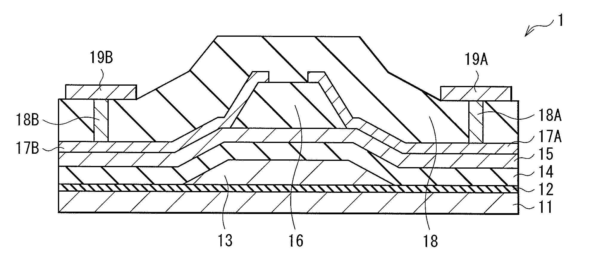
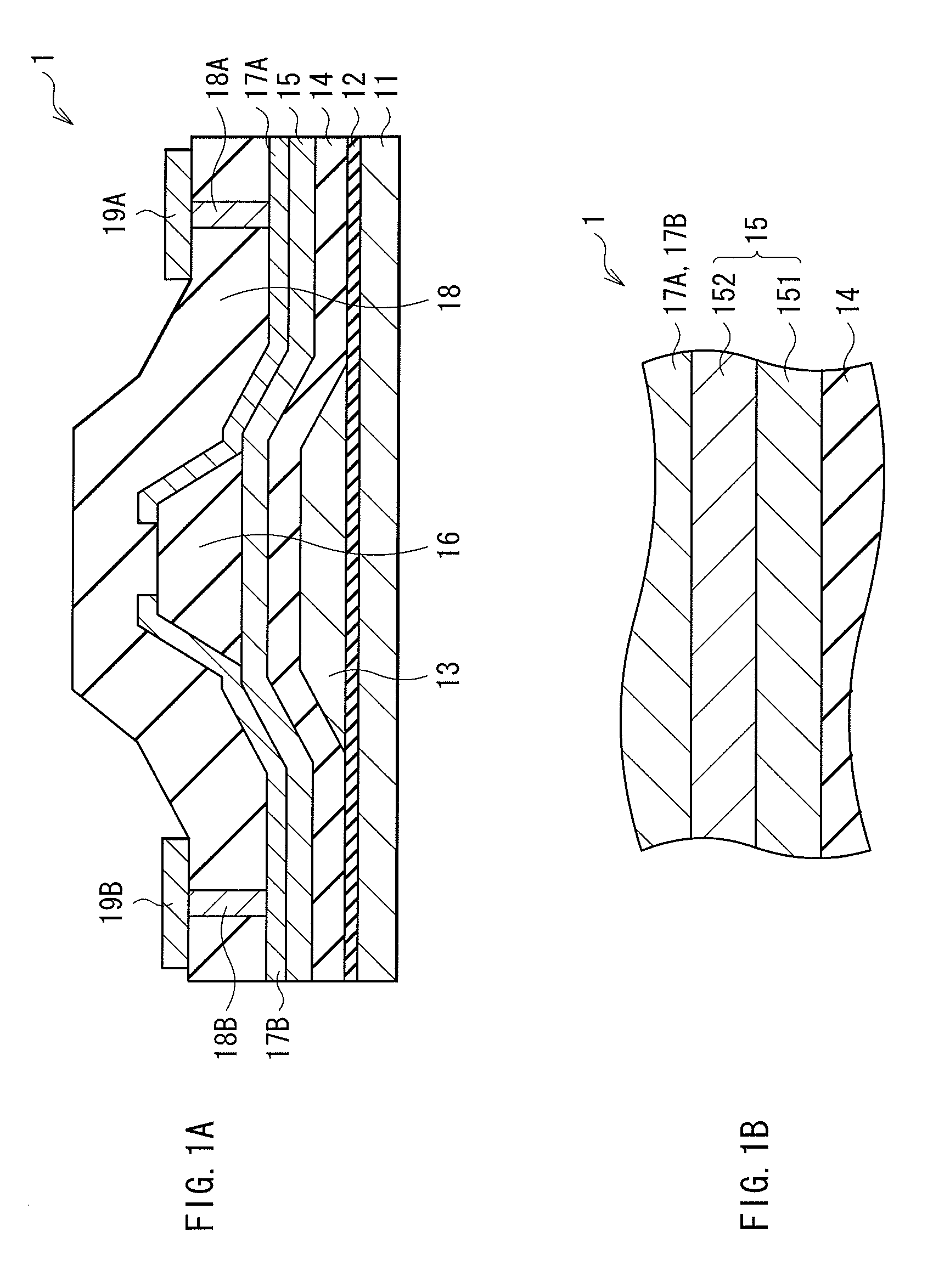
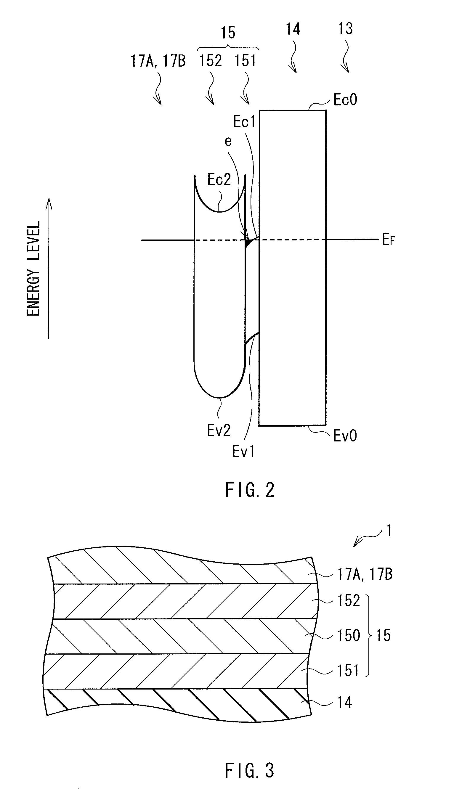
[0106]FIG. 11A shows a sectional configuration of an oxide semiconductor layer 15A of a thin film transistor (TFT 1A) according to modification 1, and FIG. 11B shows an example of an energy band structure of a layer structure around the oxide semiconductor layer 15A.

[0107]As shown in FIGS. 11A and 11B, the TFT 1A of the modification corresponds to TFT having the same configuration as that of the TFT 1 of the first embodiment except that a stacking order of the carrier travel layer 151 and the carrier supply layer 152 in the oxide semiconductor layer 15 is reversed. That is, the oxide semiconductor layer 15A of the modification is configured of a multilayer film (two-layer structure) including the carrier supply layer 152 and the carrier travel layer 151 sequentially stacked from the gate insulating film 14 side. In other words, the oxide semiconductor layer 15A includes a single heterostructure having one carrier supply layer 152 and one carrier travel layer 151 like the oxide semic...

modification 2

[0110]FIG. 12A shows a sectional configuration of an oxide semiconductor layer 15B of a thin film transistor (TFT 1B) according to modification 2, and FIG. 12B shows an example of an energy band structure of a layer structure around the oxide semiconductor layer 15B.

[0111]The TFT 1B of the modification uses holes as carriers unlike the first embodiment and the modification 1. Specifically, as shown in FIGS. 12A and 12B, the TFT 1B corresponds to the TFT having the same configuration as that of the TFT 1 of the first embodiment except that an oxide semiconductor layer 15B using holes as carriers is provided in place of the oxide semiconductor layer 15 using electrons as carriers.

[0112]The oxide semiconductor layer 15B is configured of a multilayer film (two-layer structure) including the carrier travel layer 155 and a carrier supply layer 156 sequentially stacked from a gate insulating film 14 side. In other words, the oxide semiconductor layer 15B includes a single heterostructure h...


PUM


Abstract

A thin film transistor, which is capable of improving carrier mobility, and a display device and an electronic device, each of which uses the thin film transistor, are provided. The thin film transistor includes: a gate electrode; an oxide semiconductor layer including a multilayer film including a carrier travel layer configuring a channel and a carrier supply layer for supplying carriers to the carrier travel layer; a gate insulating film provided between the gate electrode and the oxide semiconductor layer; and a pair of electrodes as a source and a drain. A conduction band minimum level or a valence band maximum level corresponding to a carrier supply source of the carrier supply layer is higher in energy than a conduction band minimum level or a valence band maximum level corresponding to a carrier supply destination of the carrier travel layer.

Description

BACKGROUND OF THE INVENTION[0001]1. Field of the Invention[0002]The present invention relates to a thin film transistor (TFT) using an oxide semiconductor layer, and a display device and an electronic device, each of which uses such a thin film transistor.[0003]2. Description of Related Art[0004]In a flat panel display such as a liquid crystal display or an organic EL (Electro Luminescence) display, a silicon (Si) material is typically used for a channel layer (active layer) of a driving thin-film transistor. Specifically, for example, amorphous Si or polycrystalline Si is used.[0005]However, in the case of using amorphous Si for the channel layer, while a display is easily increased in size, since carrier (for example, electron) mobility is low, about 1 cm2 / V*s or less, display performance has been hardly improved. On the other hand, in the case of using polycrystalline Si for the channel layer, while carrier mobility is high, about 30 to 300 cm2 / V*s, a display has been hardly incr...

Claims


Application Information

Patent Timeline
Patent Type & Authority Patents(United States)
IPC IPC(8): H01L29/786
CPCH01L29/7869H01L29/78693
Inventor TANIGUCHI, SATOSHIYOKOZEKI, MIKIHIROMIYASHITA, HIROKOSUZUKI, TOSHI-KAZU
Owner JOLED INC
Why Eureka
Try Eureka