

Tunneling transistor suitable for low voltage operation
a technology of tunneling transistor and low voltage, which is applied in the direction of superconductor devices, electrical apparatus, semiconductor devices, etc., can solve the problem of limited maximum integration density of modern integrated circuits
- Summary
- Abstract
- Description
- Claims
- Application Information
AI Technical Summary
Benefits of technology
Problems solved by technology
Method used
Image

Examples
Embodiment Construction
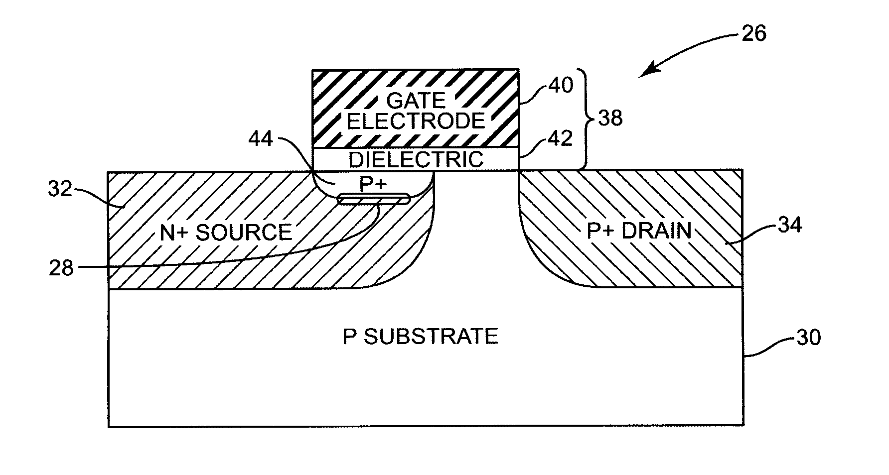
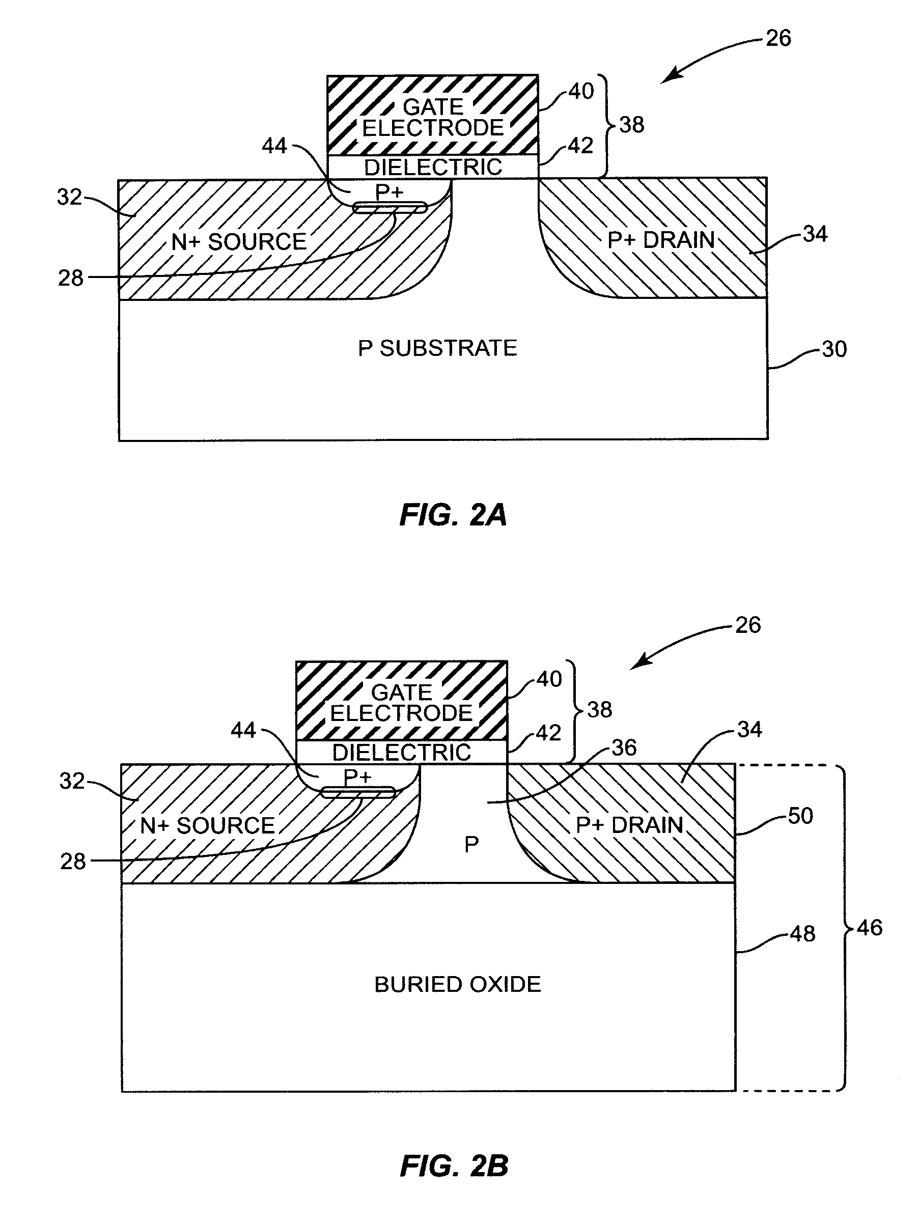
[0007]Several embodiments of a tunneling transistor are disclosed. In one embodiment, a tunneling transistor includes a semiconductor substrate, a source region formed in the semiconductor substrate, a drain region formed in the semiconductor substrate, a gate stack including a metallic gate electrode and a gate dielectric, and a tunneling junction that is substantially parallel to an interface between the metallic gate electrode and the gate dielectric. As a result of the tunneling junction that is substantially parallel with the interface between the metallic gate electrode and the gate dielectric, an on-current of the tunneling transistor is substantially improved as compared to that of a conventional tunneling transistor.
[0008]In one embodiment, a tunneling transistor includes a semiconductor substrate, a source region formed in the semiconductor substrate, a drain region formed in the semiconductor substrate, and a gate stack that overlaps a portion of the source region and inc...
PUM
 Abstract
Description
Claims
Application Information