

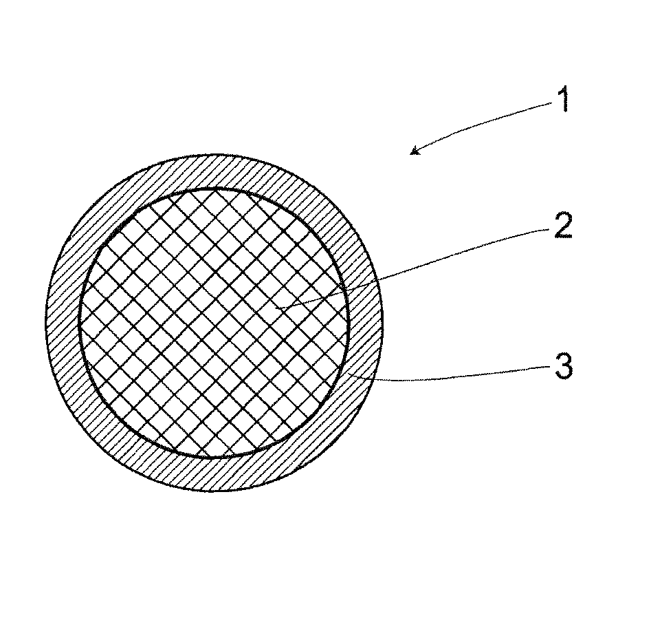
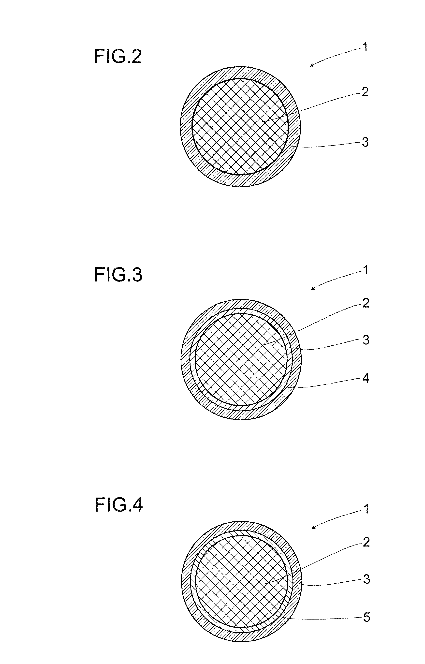
Bonding wire for semiconductor devices
a technology of semiconductor devices and bonding wires, which is applied in the direction of insulated conductors, power cables, cables, etc., can solve the problems of difficult to comprehensively satisfy the various characteristics requisite for bonding wires, reduced bonding strength, and high risk of corrosion of the wire surface, so as to promote the stabilization of the bonded shape of the bonding wire, reduce damage at the neck part, and improve the linearity of the loop and the stability of the loop heigh
- Summary
- Abstract
- Description
- Claims
- Application Information
AI Technical Summary
Benefits of technology
Problems solved by technology
Method used
Image

Examples
examples
[0101]An explanation will be given of examples of the present invention.
[0102]As raw materials for bonding wires, Cu, Au, and Ag which were to be used for a core member and which had a high purity of greater than or equal to approximately 99.99% by weight were prepared, and Au, Pt, Pd, Ru, and Rh which had a purity greater than or equal to 99.99% by weight and which were to be used for a skin layer or an intermediate metal layer were also prepared.
[0103]Wires thinned to a certain wire diameter were used as a core member, and electrolytic plating, nonelectrolytic plating, vapor deposition, melting and the like were performed thereon and a thermal treatment was performed to form a different metal layer on a wire surface of the core member. A method of forming a skin layer at a final wire diameter and a method of forming a skin layer at a certain wire diameter and of thinning a wire to a final wire diameter by wire drawing were adopted. Commercially-available plating solutions for a se...
PUM
| Property | Measurement | Unit |
|---|---|---|
| thickness | aaaaa | aaaaa |
| diameter | aaaaa | aaaaa |
| thickness | aaaaa | aaaaa |
Abstract
Description
Claims
Application Information