
Substrate transfer apparatus and substrate treatment system
a technology of substrate treatment and transfer apparatus, which is applied in the direction of conveyors, manufacturing tools, instruments, etc., can solve the problems of reducing the yield of products manufactured by the substrate treatment system, and non-negligent problems, so as to increase the flow speed of gas, reduce the substrate, and raise the substrate
- Summary
- Abstract
- Description
- Claims
- Application Information
AI Technical Summary
Benefits of technology
Problems solved by technology
Method used
Image

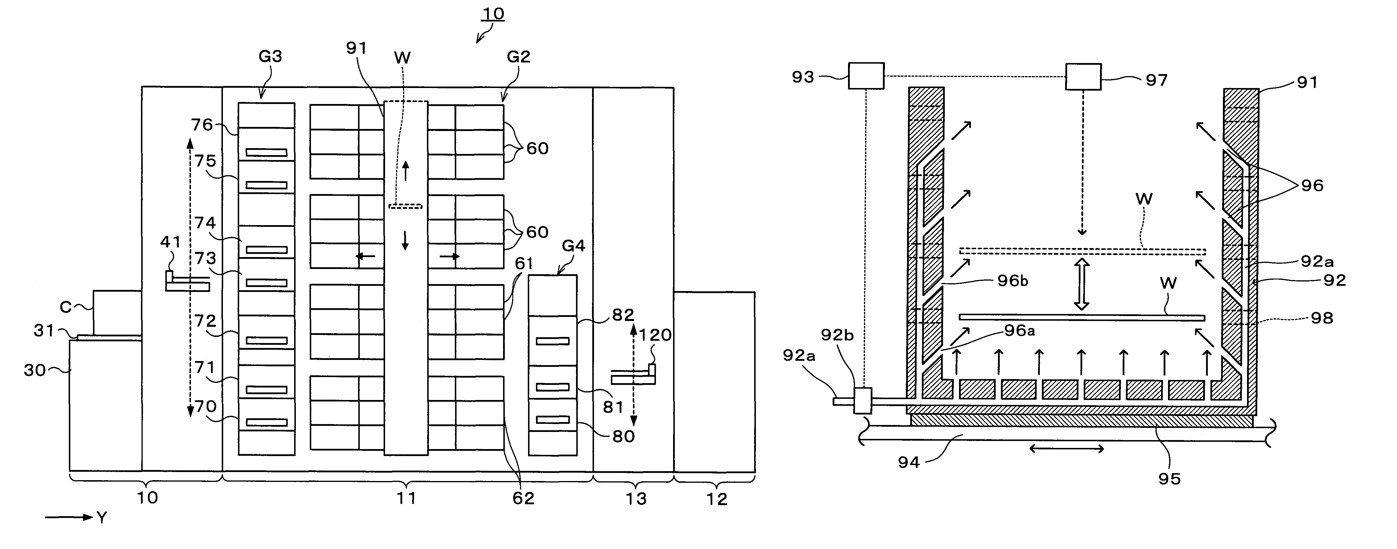
Examples
Embodiment Construction
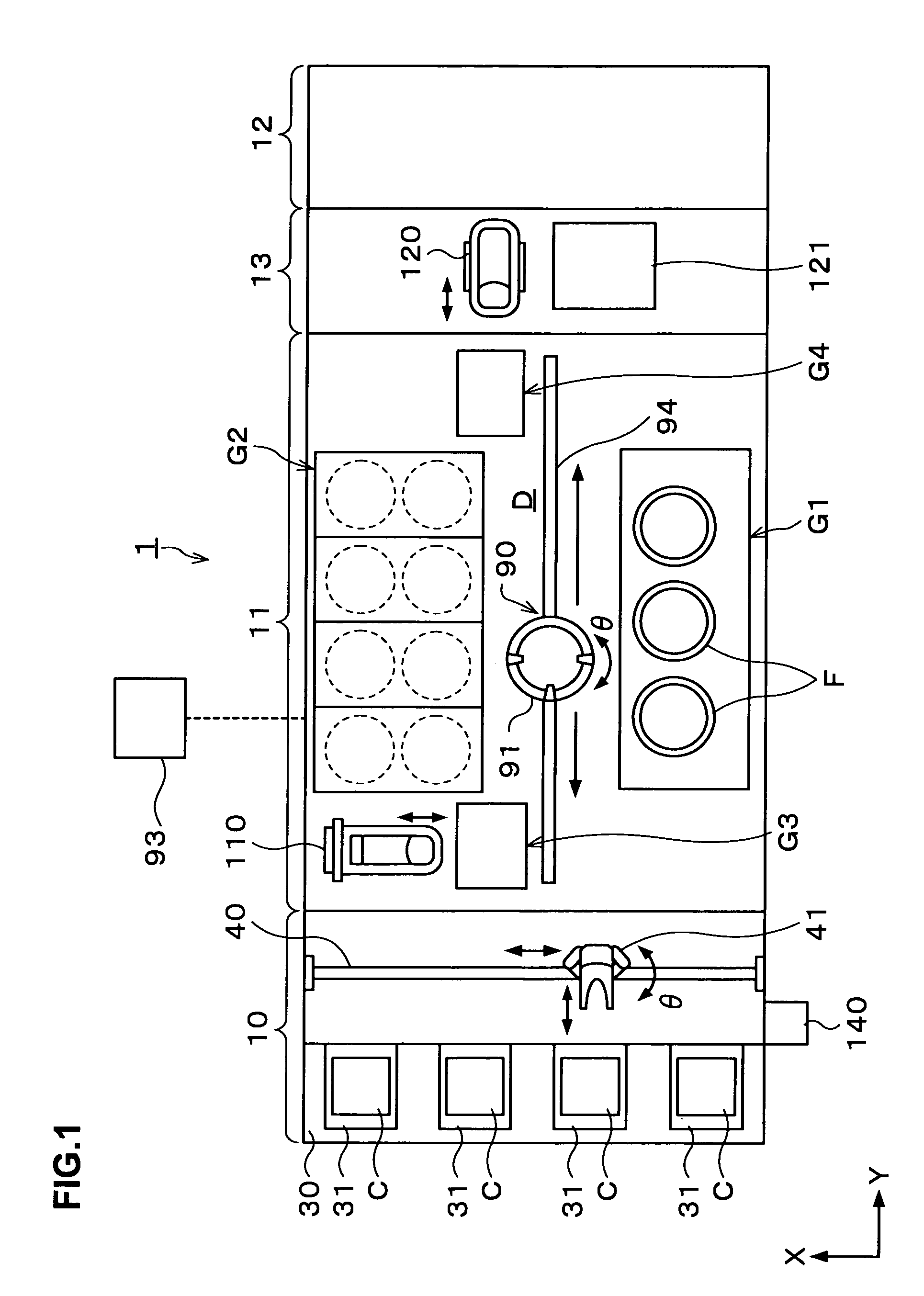
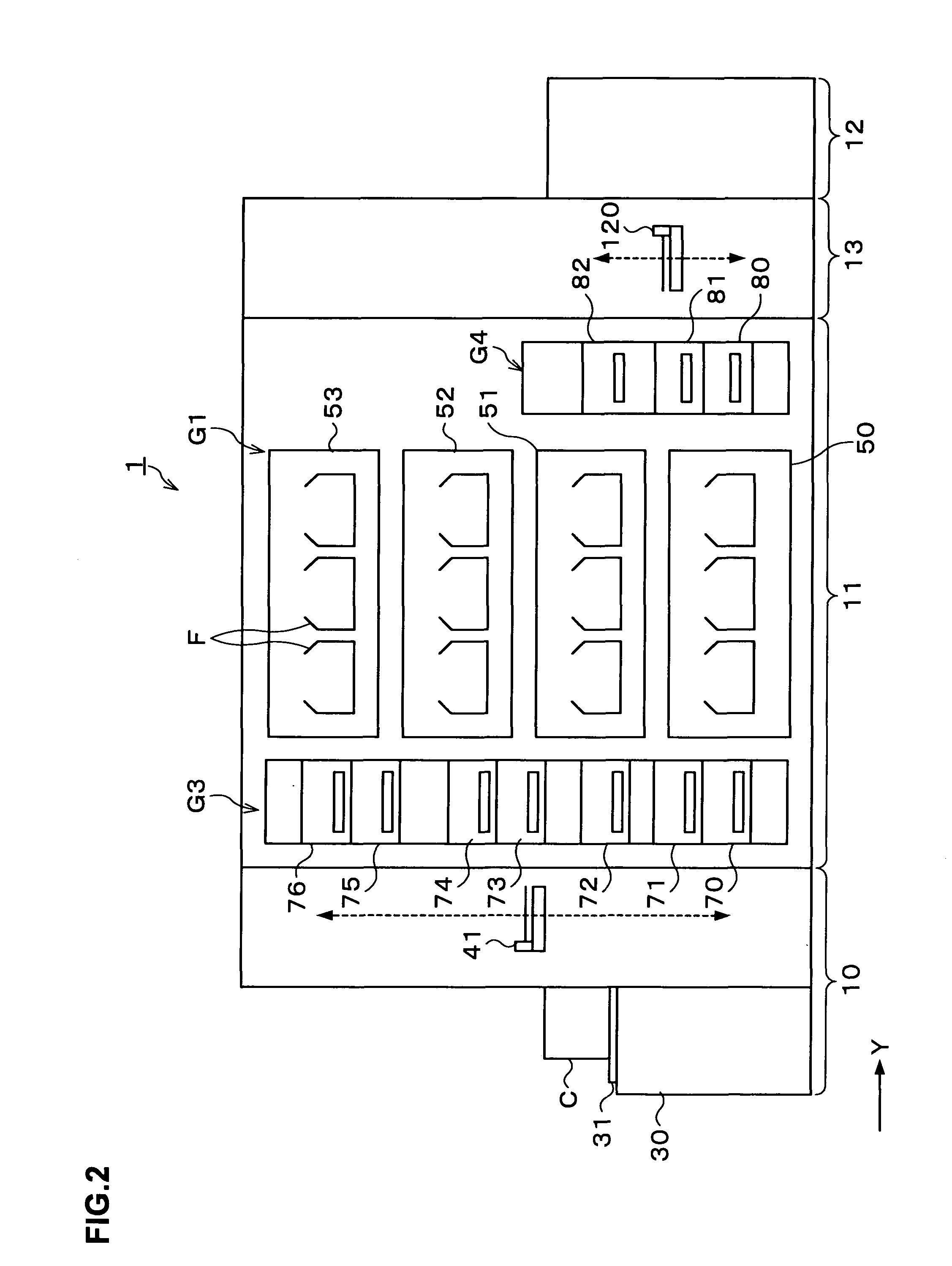
[0031]Hereinafter, embodiments of the present invention will be described. FIG. 1 is an explanatory view showing the outline of a structure of a coating and developing treatment system 1 according to the present invention.
[0032]The coating and developing treatment system 1 has, as shown in FIG. 1, a structure in which, for example, a cassette station 10 into / from which cassettes C are transferred from / to the outside; a treatment station 11 including a plurality of various kinds of treatment apparatuses each for performing predetermined treatment in a manner of single-substrate treatment in photolithography processing; and an interface station 13 for delivering the substrate W to / from an aligner 12 adjacent to the treatment station 11, are integrally connected. Note that in this embodiment, for example, a semiconductor wafer is used as the substrate W.
[0033]In the cassette station 10, a cassette mounting table 30 is provided. On the cassette mounting table 30, a plurality of, for exa...
PUM
| Property | Measurement | Unit |
|---|---|---|
| height | aaaaa | aaaaa |
| circumference | aaaaa | aaaaa |
| circular shape | aaaaa | aaaaa |
Abstract
Description
Claims
Application Information