Apparatus and method for etching semiconductor wafer

a technology of etching apparatus and semiconductor wafer, which is applied in the direction of semiconductor/solid-state device manufacturing, electric apparatus, basic electric elements, etc., can solve the problems of affecting the etching effect of the semiconductor wafer. , to achieve the effect of suppressing the evaporation of the etchant, preventing the splash of the etchan

Inactive Publication Date: 2010-02-04
SUMCO CORP
View PDF4 Cites 3 Cited by
  • Summary
  • Abstract
  • Description
  • Claims
  • Application Information

AI Technical Summary

Benefits of technology

[0014]According to the present invention, the outside diameter of the etching bath is set to be not more than the outside diameter of the semiconductor wafer and, therefore, during etching, the whole liquid surface of the etching bath is covered with the semiconductor wafer. For this reason, even when vibrations occur in the semiconductor wafer held by the Bernoulli chuck, the effect of the vibrations on the liquid surface is small and, therefore, the splash of the etchant can be prevented. Also, the evaporation surface of the etchant is limited to a portion of the liquid surface of the etchant overflowing from a gap between the etching bath and the surface of the wafer to be etched and, therefore, it is possible to suppress the evaporation of the etchant. Therefore, it is possible to prevent the non-etched region of the semiconductor wafer from deteriorating due to the splash of the etchant and the evaporation of the etchant. The outside diameter of the etching bath may be equal to the outside diameter of the semiconductor wafer or may be smaller than the outside diameter of the semiconductor wafer. However, in order to reduce the effect of the splash of the etchant and the vapor of the etchant to a smaller extent, it is more preferred that the outside diameter of the etching bath be smaller than the outside diameter of the semiconductor wafer.
[0015]In this case, the Bernoulli chuck is provided with an annular gas supply port which sends gas to the side of an outer circumferential portion of one surface of the semiconductor wafer. Because of this, it is possible to prevent the vapor of the etchant from intruding on the side of one surface of the semiconductor wafer and, therefore, it is possible to more reliably prevent the deterioration of the non-etched region of the semiconductor wafer.
[0016]The apparatus for etching a semiconductor wafer of the present invention also includes a storage bath which stores the etchant which overflows the etching bath, and circulation means which extracts the etchant in the storage bath by a pump and returns the etchant to the supply port. By using the etchant in a circulating manner like this, it is possible to continuously maintain the liquid surface in the etching bath at a certain height and it is possible to reduce the process cost by reducing etchant waste.
[0017]The etching bath has an inner wall surface which spreads in the form of an inverted cone from a circumference of the supply port toward an upper end of the etching bath. Because of this, for example, the etchant supplied from the supply port into the etching bath flows so as to spread from the center in the radial direction along the inner surface wall and, therefore, the stagnation of the etchant in the bath is suppressed, making it possible to form a flow of the liquid without turbulence. As a result of this, when the semiconductor wafer has come into contact with the etchant, the region in which the etchant and the semiconductor wafer are in contact with each other expands smoothly in the circumferential direction. For this reason, the outer circumferential portion of the semiconductor wafer is uniformly in contact with the liquid surface in the circumferential direction and hence it is possible to suppress nonuniform etching.
[0018]In an etching method for etching a semiconductor wafer by use of an etching apparatus in which the outside diameter of an etching bath is set, at least either a set height of the surface of the semiconductor wafer to be etched or a supply amount of the etchant supplied from the supply port is adjusted and the etchant is brought into contact with a prescribed position of an outer circumferential portion of the semiconductor wafer. That is, a set height of the surface of the semiconductor wafer to be etched and a supply amount of the etchant supplied from the supply port are adjusted, whereby the surface tension acting on the etchant passing between the top end surface of the etching bath and the surface of the semiconductor wafer to be etched changes. The position of the liquid surface depends on the magnitude of the surface tension. Therefore, by appropriately adjusting a set height of the surface of the semiconductor wafer to be etched and a supply amount of the etchant supplied from the supply port, it becomes possible to adjust the region in which the etchant comes into contact with the semiconductor wafer within an appropriate range.
[0019]According to the present invention, it is possible to prevent the splash of an etchant when one surface of a wafer is etched, with the wafer held by use of a Bernoulli chuck.

Problems solved by technology

However, if such holding means is used, particles are likely to adhere to the front surface side of the wafer.
However, in this Bernoulli chuck, chattering associated with the flow of a suction gas is likely to occur in the wafer.
If the etchant is splashed, the etchant will adhere to the non-etched region of the wafer and might deteriorate the surface.

Method used


Image

  • Apparatus and method for etching semiconductor wafer
  • Apparatus and method for etching semiconductor wafer
  • Apparatus and method for etching semiconductor wafer

Examples


Embodiment Construction

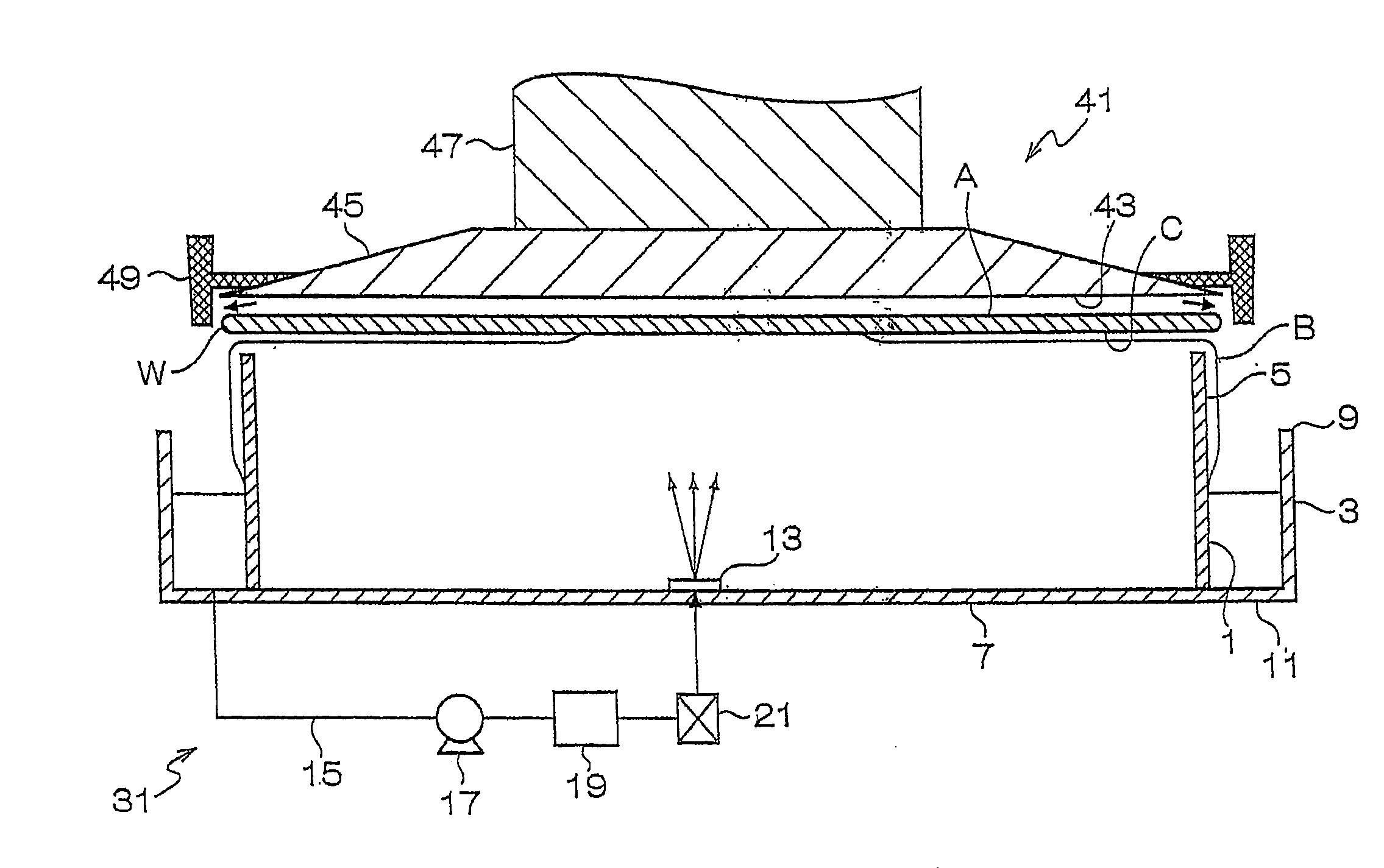
[0025]Hereinafter, embodiments of an etching apparatus for a semiconductor wafer to which the present invention is applied will be described with reference to the drawings.

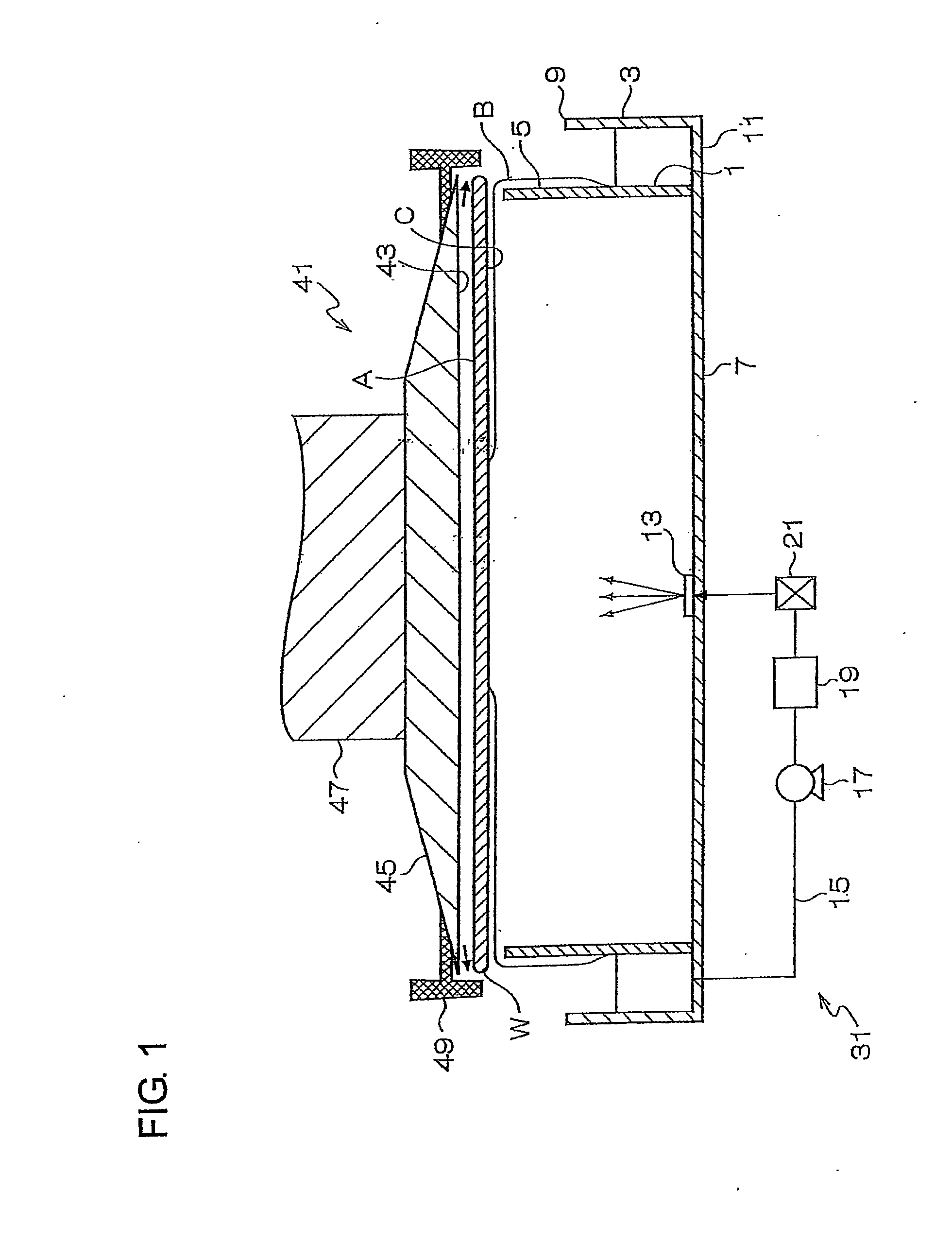
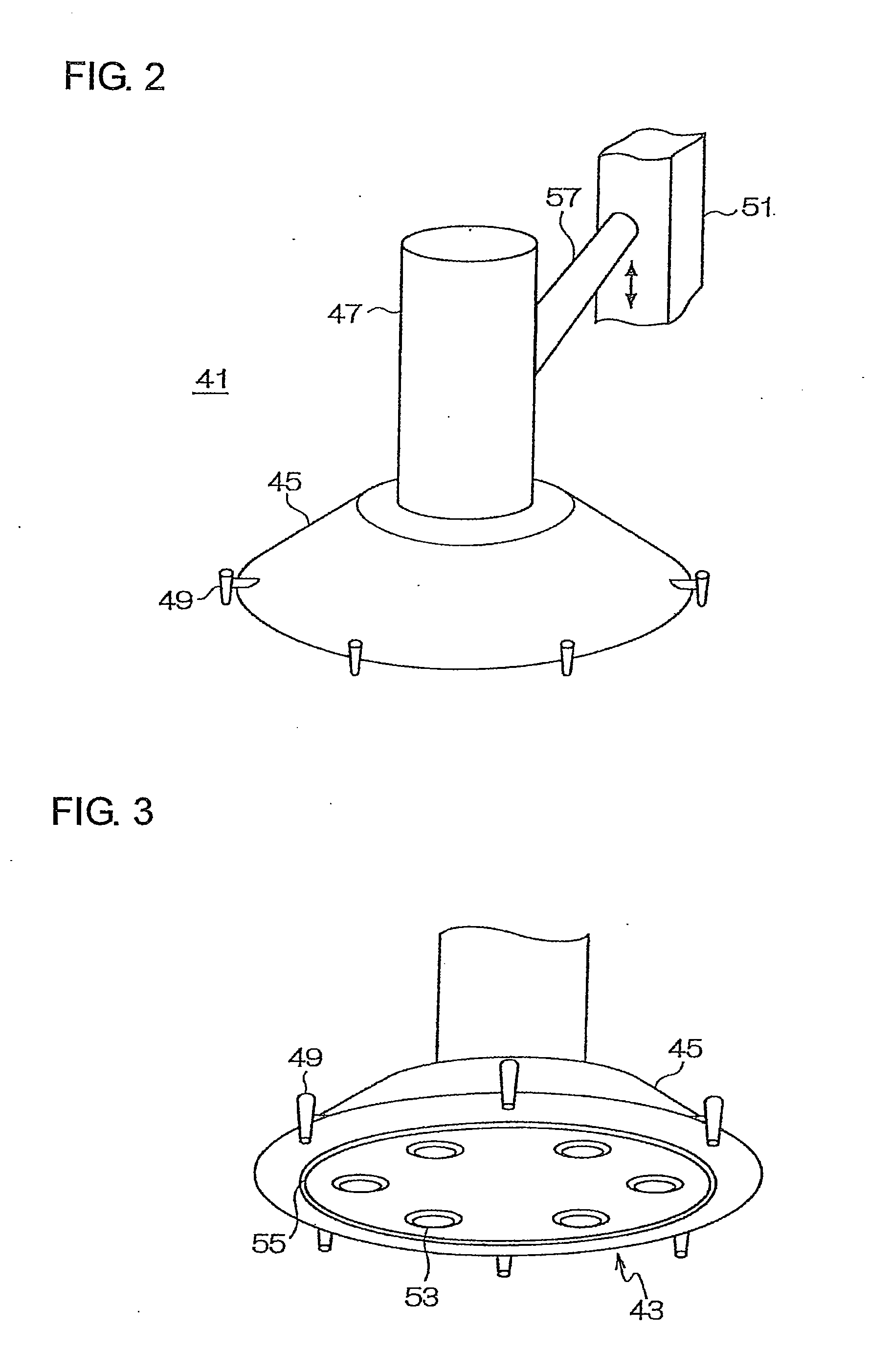
[0026]FIG. 1 is a longitudinal sectional view showing the general arrangement of an etching apparatus to which the present invention is applied. FIG. 2 is a perspective view showing the appearance of a Bernoulli chuck of the etching apparatus to which the present invention is applied. FIG. 3 is an enlarged perspective view of a wafer holding portion of the Bernoulli chuck of the etching apparatus to which the present invention is applied. FIGS. 4(a) to 4(c) are diagrams to explain the operation of the etching apparatus to which the present invention is applied.

[0027]In this embodiment, semiconductor wafers can include a silicon wafer, a gallium arsenide wafer and the like. However, a SIMOX wafer after heat treatment (hereinafter, abbreviated as “wafer”) will be described here. In the outer circumferential portion ...


PUM

PropertyMeasurementUnit
heightaaaaaaaaaa
diameteraaaaaaaaaa
circumferenceaaaaaaaaaa

Abstract

An apparatus for etching a semiconductor wafer of the present invention includes a cylindrical inner bath 1 which stores an etchant, a blow-off nozzle 13 which supplies the etchant from a middle part of a bottom surface 7 of the inner bath 1 toward a middle part of a liquid surface of the etchant, a Bernoulli chuck 41 which holds one surface of the semiconductor wafer W in a noncontact manner, and raising and lowering means 51 which is capable of descending, while keeping the semiconductor wafer W horizontal, to a set height at which the other surface of the semiconductor wafer W to be etched comes into contact with the liquid surface. The inner bath 1 is formed in such a manner that the outside diameter of the inner bath 1 is not more than the outside diameter of the semiconductor wafer W. As a result of this, it is possible to prevent the splash of the etchant when one surface of the wafer is etched, with the wafer held by use of the Bernoulli chuck.

Description

BACKGROUND OF THE INVENTION[0001]1. Field of the Invention[0002]The present invention relates to an apparatus and method for etching a semiconductor wafer.[0003]2. Description of the Related Art[0004]In the manufacturing process of semiconductor wafer, high-temperature heat treatment (annealing) is repeatedly performed during the steps of, for example, oxidation, diffusion, film formation and the like. In the manufacturing process of, for example, SIMOX wafers, heat treatment is performed in a high-temperature oxidizing atmosphere, with the silicon wafer held by a heat treatment jig made of silicon or made of silicon carbide (SiC).[0005]Incidentally, when heat treatment is repeated in the oxidizing atmosphere, an oxide film grows on the surface of the heat treatment jig and part of the oxide film may be transferred to a holding surface (hereinafter referred to as the back surface) of a semiconductor wafer which comes into contact with the heat treatment jig.[0006]An oxide (i.e. the ...

Claims


Application Information

Patent Timeline
Patent Type & Authority Applications(United States)
IPC IPC(8): H01L21/306C23F1/08
CPCH01L21/0209H01L21/6838H01L21/67086
Inventor OKITA, KENJI
Owner SUMCO CORP
Why Eureka
Try Eureka