Semiconductor device and multilayer semiconductor device

a semiconductor and semiconductor technology, applied in the field of semiconductor devices, can solve the problems of not being able to allocate consecutively numbered chip identifiers to different semiconductor chips, complicating circuit configuration, and ensuring the setting of chip identifiers, etc., and achieve excellent effects

Active Publication Date: 2013-03-26
TESSERA ADVANCED TECH
View PDF10 Cites 22 Cited by
  • Summary
  • Abstract
  • Description
  • Claims
  • Application Information

AI Technical Summary

Benefits of technology

[0027]As described above and according to the embodiments of the disclosure, excellent effects are provided that the number of wires of semiconductor chips to be made common for the setting of chip identifiers can be reduced to one.

Problems solved by technology

The third technology mentioned above includes a technique that can automatically set chip identifiers by an internal circuit, but, because chip identifiers are determined depending on an uncertain reason, namely, variations in manufacturing, cannot always guarantee the setting of the chip identifiers that are unique to different semiconductor chips.
In addition, this technology may not allocate consecutively numbered chip identifiers to different semiconductor chips.
Therefore, a circuit of reading the chip identifiers of semiconductor chips by a controller for example has to be added, thereby complicating the circuit configuration.
However, if the semiconductor chips have different structures, achieving the commonality of the number of wires in correspondence with the setting of chip identifiers requires the sufficient consideration of the setting of the positional relationships with other wires, for example, thereby making it difficult to implement this technology.
This problem becomes more conspicuous as the number of wires between the increment circuits increases in correspondence with the increase in the number of semiconductor chips to be layered.

Method used


Image

  • Semiconductor device and multilayer semiconductor device
  • Semiconductor device and multilayer semiconductor device
  • Semiconductor device and multilayer semiconductor device

Examples


first embodiment

(1) First Embodiment

An Overall Configuration of a Multilayer Semiconductor Device

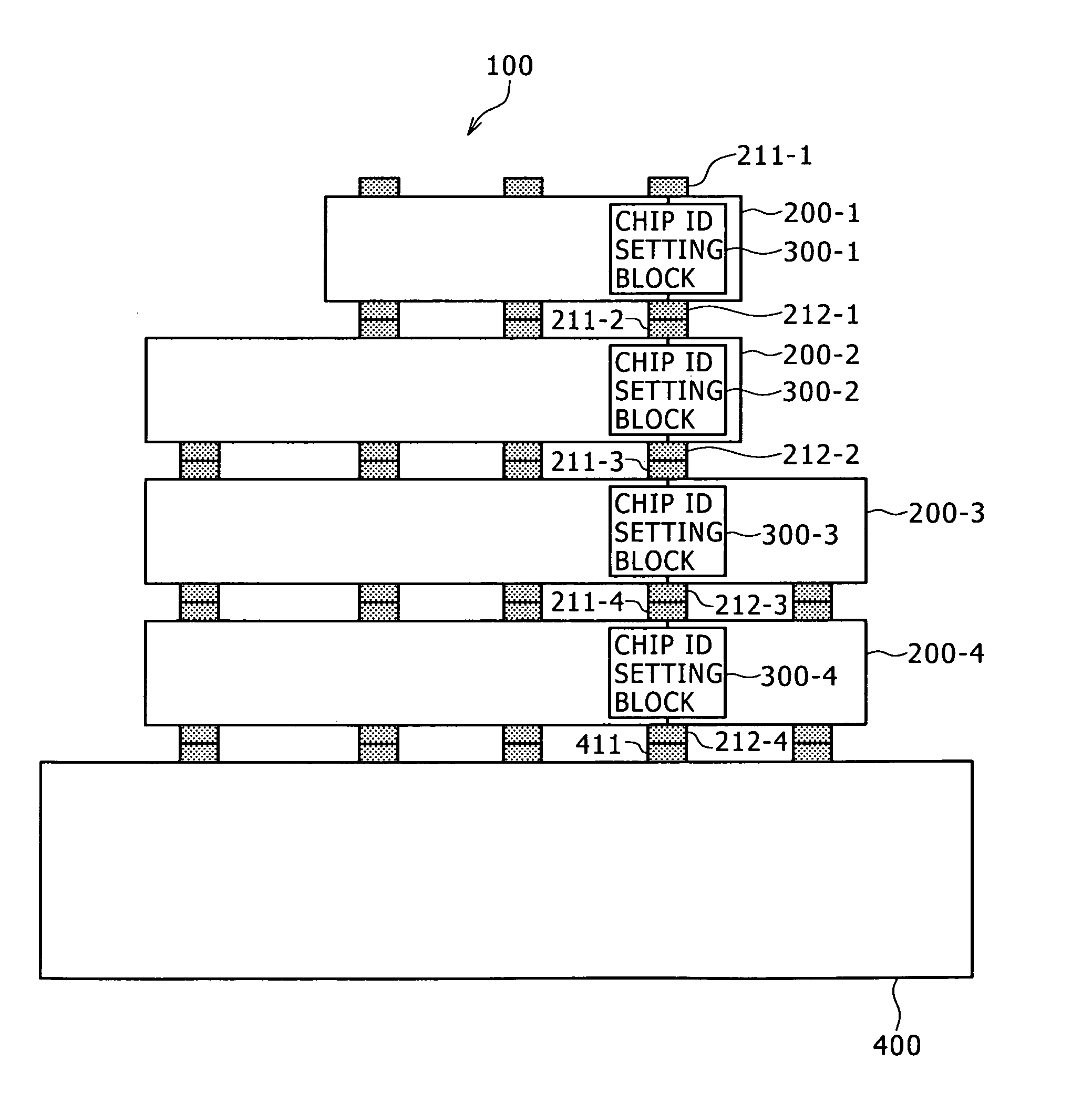
[0047]Now, referring to FIG. 1, there is shown an exemplary configuration of a multilayer semiconductor device 100 practiced as the first embodiment of the disclosure. The multilayer semiconductor device 100 shown in the figure has a structure in which chips 200-1, 200-2, 200-3, and 200-4 and a base chip 400 are layered from top to bottom in this order. The chips 200-1 to 200-4 are semiconductor chips each having a predetermined function. It should be noted that the chips 200-1 to 200-4 have not especially a common structure; namely, these chips have different structures in accordance with the functions assigned thereto.

[0048]The base chip 400 is arranged at the bottom of the multilayer semiconductor device 100. Signals for controlling the chips 200-1 to 200-4 are outputted from the base chip 400 for example to be transmitted to the chips 200-1 to 200-4 via predetermined wires between the chip layers, f...

second embodiment

(2) Second Embodiment

Exemplary Configuration of a Chip Identifier Setting Block

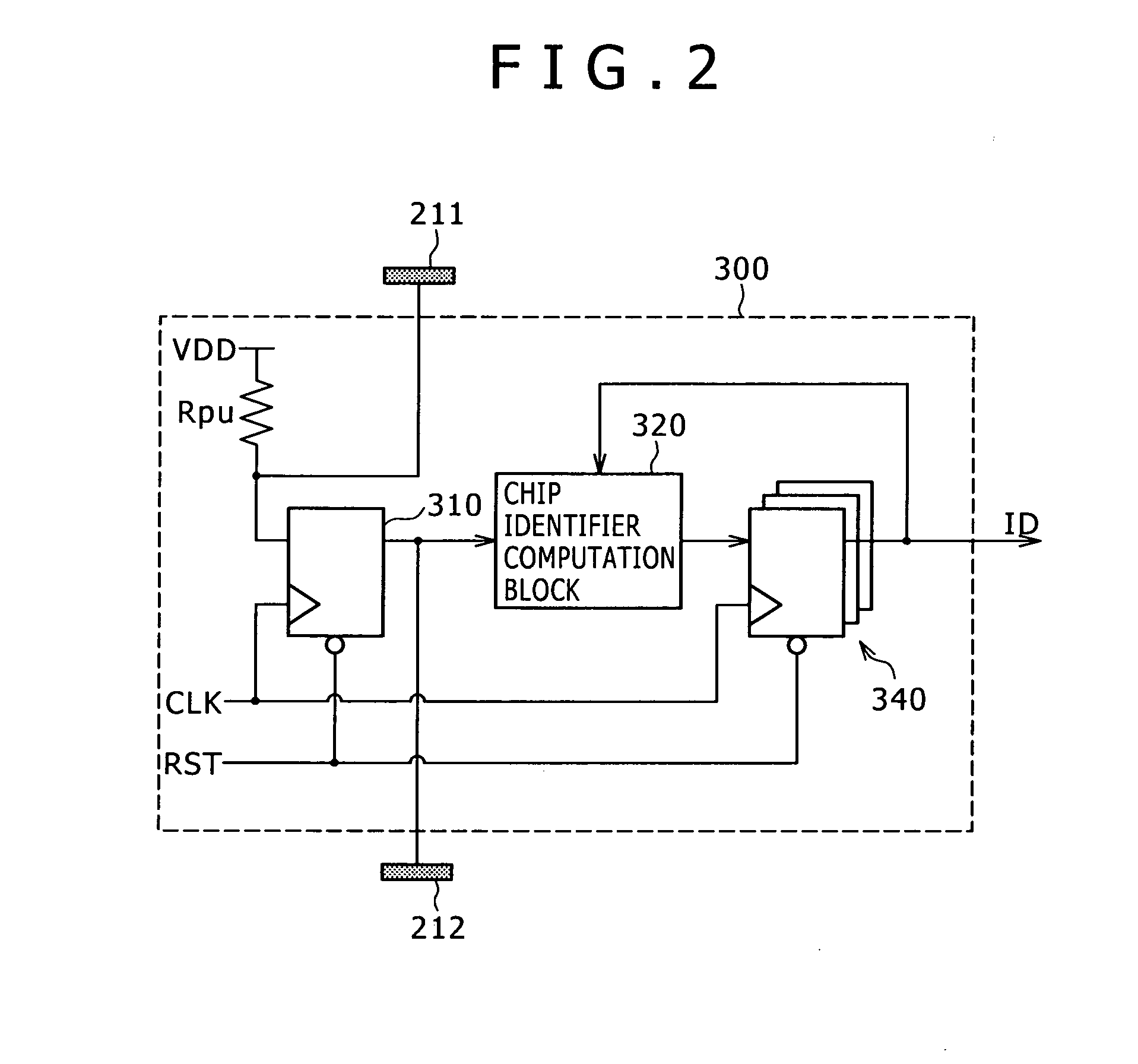
[0089]The following describes the second embodiment of the disclosure. The first embodiment described above provides a basic configuration for assigning consecutive chip identifiers ID in the ascending order from “1” and the shift register block 310 in each chip identifier setting block 300 is a one-bit shift register.

[0090]By contrast, in the second embodiment, the shift register block 310 is configured as a multiple-bit shift register of two or more bits. By use of this configuration, chip identifiers ID are set to each chip 200 as with the first embodiment and data indicative of the content of predetermined information associated with the each chip 200 is transmitted to the base chip 400 (refer to FIG. 1). It should be noted that the data indicative of the content of predetermined information associated with each chip 200 is hereafter referred to as chip-associated data.

[0091]The above-mentioned chip-a...

third embodiment

(3) Third Embodiment

Exemplary Configuration of the Chip

[0121]The following describes the third embodiment of the disclosure. For the chip 200 corresponding to the third embodiment, a chip with a memory block internally installed is assumed, for example. An actual memory block may include a DRAM (Dynamic Random Access Memory), an SRAM (Static Random Access Memory), or a flash memory, for example. It is also assumed that the memory block be formed by one or more memory planes. A memory plane denotes a storage area obtained by logically dividing the memory block. It is also assumed that the size of the memory planes be common to the memory blocks of the chips. It should be noted that the number of memory planes forming a memory block need not be the same between the memory blocks of the chips; that is, different chips 200 may have the different number of memory planes.

[0122]In a multiplayer semiconductor device with the chips 200 layered as described above, access is executed by specif...


PUM


Abstract

Disclosed herein is a semiconductor device including: an input terminal receiving, if a preceding-stage semiconductor device is layered on a predetermined one of an upper layer and a lower layer, a bit train outputted from the preceding-stage semiconductor device; a semiconductor device identifier hold block holding a semiconductor device identifier for uniquely identifying the semiconductor device; a semiconductor device identifier computation block executing computation by using the semiconductor device identifier to update the semiconductor device identifier held in the semiconductor device identifier hold block according to a result of the computation; a control block once holding data of a bit train entered from the input terminal to control updating of the semiconductor device identifier executed by the semiconductor device identifier computation block based on the held data; and an output terminal outputting the bit train held in the control block to a succeeding-stage semiconductor device layered on another layer.

Description

BACKGROUND[0001]The present disclosure relates to a semiconductor device and, more particularly, to a semiconductor device in which a semiconductor identifier is set after layering in a multilayer semiconductor device and a multilayer semiconductor device formed by layering two or more such semiconductor devices.[0002]For an integrated semiconductor device, a multilayer semiconductor device formed by layering two or more semiconductor chips for three-dimensional configuration is known. The semiconductor chips layered in such a multilayer semiconductor device are interconnected with common wiring, such as a bus, for example. This common wiring is hereafter referred to also as global wiring.[0003]When global wiring is employed, control signals generated by a logic and the like are simultaneously transmitted to two or more semiconductor chips via global wiring. Therefore, selective access to one specific semiconductor chip requires for this semiconductor chip to recognize whether or no...

Claims


Application Information

Patent Timeline
Patent Type & Authority Patents(United States)
IPC IPC(8): H01L23/48
CPCG11C8/12G11C16/20H01L23/544H01L25/0657H01L24/16H01L24/17H01L2223/5444H01L2224/16145H01L2224/17181H01L2225/06513
Inventor IMAI, MAKOTO
Owner TESSERA ADVANCED TECH
Why Eureka
Try Eureka