
Method to linearize the output from an ADC

a technology of linearization and output, applied in the field of analogtodigital converters, can solve the problems of insufficient testing to measure adcs with dynamic errors like hysteresis, exposure of wide-band receivers, and degradation of linearity

Inactive Publication Date: 2013-04-02
NXP BV
View PDF10 Cites 10 Cited by
  • Summary
  • Abstract
  • Description
  • Claims
  • Application Information

AI Technical Summary

Benefits of technology

The present invention provides a method for compensating the output of an ADC for non-linearity by applying a vector of correction factors to each of a block of uncorrected ADC output samples, to provide a block of corrected ADC samples. The method iteratively minimizes a measure of the spectral flatness of the block of corrected ADC samples with respect to the vector of correction variables. This technique overcomes the disadvantages associated with conventional linearization methods and enhances the accuracy and reliability of the measurement process.

Problems solved by technology

In addition, such a wide band receiver may be exposed to the “near-far problem” in that it may receive signals from antennas at widely different distances from the receiver: the ADC should be capable of digitising signals from both the distant and nearby antenna accurately.
In particular, deviations in the actual resistance or capacitance values of manufactured on-chip components such as resistors or capacitors, from the design values, can directly result in non-linearity.
These deviations can easily arise due to IC process spread, moreover currents which exceed the (small signal) approximations of transistors may also degrade the linearity.
However, such tests are inadequate to measure ADCs with dynamic errors like hysteresis.
However, these methods require precise knowledge of the input frequency which also needs to fall on the grid of fast Fourier transform (FFT) frequencies corresponding to the sine wave input.

Method used


Image

  • Method to linearize the output from an ADC
  • Method to linearize the output from an ADC
  • Method to linearize the output from an ADC

Examples


Embodiment Construction

[0032]The ADC output signal during a training phase has a finite length; that during the operational phase has a semi-infinite length. For a block of samples of the signal x(k), k=0, 1, . . . , the vector notation {right arrow over (x)}=(x0, x1, . . . , xN−1) will be used. The corresponding fast Fourier transform (FFT) spectrum is denoted {right arrow over (X)}=(X0, X1, . . . , XN−1). δ(k) is the Kronecker delta function, such that δ(k)=0, except for δ(0)=1.

[0033]We assume that the impulse response h(k) of the ΣΔ-loop filter satisfies h(k)=0 for k=0, −1, . . . due to causality and a minimal one unit delay in the loop. Truncate the estimate of h to at most P non-zero (complex) samples, such that

h(k)=0 for k=P+1, P+2 . . . .

[0034]The transfer function of the loop is denoted H=FFTN(h).

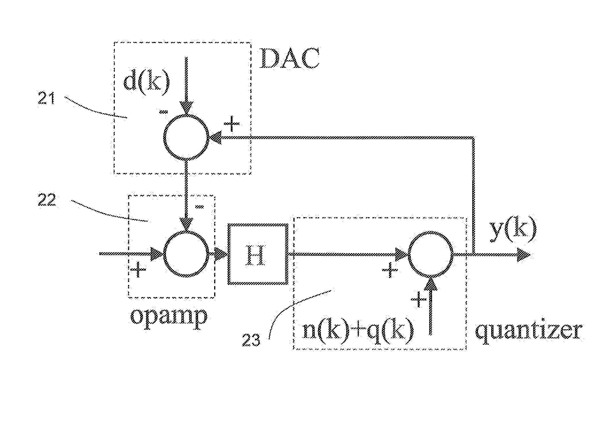
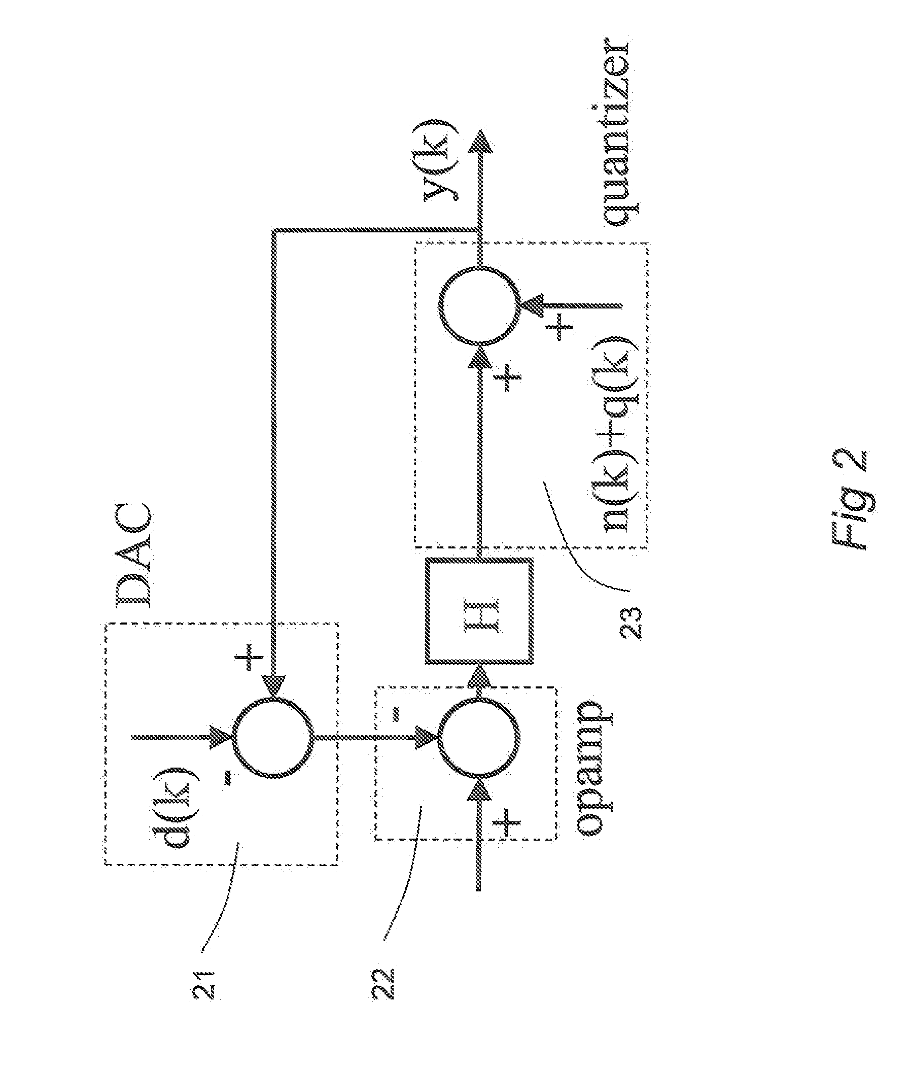
[0035]FIG. 2 depicts the additive errors due to mismatch in the quantizer and DAC inside a ΣΔ feedback loop.

[0036]In FIG. 2 the DAC 21 introduces, negatively, an error d(k); this error is fed through the ...


PUM


Abstract

A method is disclosed of compensating the output of an ADC for non-linearity in the response of the ADC. The method comprises converting an analog input signal to uncorrected digital ADC output samples, applying a vector of correction variables to each of a block of uncorrected ADC output samples to provide a block of corrected ADC samples, and iteratively minimizing a measure of the spectral flatness of the block of corrected ADC samples with response to the vector of correction variables.

Description

FIELD OF THE INVENTION[0001]This invention relates to analog-to-digital converters (ADC), and in particular to methods for linearizing the corrected output from such ADCs.BACKGROUND OF THE INVENTION[0002]The analog-to-digital converter is a class of electronic component which is used in a wide variety of applications ranging from instrumentation to communications. The basic function of an ADC is to accept an input which is analog—that is to say, it can have any of a continuous range of values—and provide an output in a digital form—that is to say, the output must lie within a representation of a subset of the natural numbers.[0003]In order to properly carry out their function, the vast majority of ADCs are required to be as nearly as possible, or at least approximately, linear: the output should be directly proportional to the input.[0004]An example of an ADC which requires high linearity is that for a single frequency modulated (FM) radio signal, which requires to be linear over th...

Claims


Application Information

Patent Timeline
Patent Type & Authority Patents(United States)
IPC IPC(8): H03M1/06
CPCH03M3/386H03M3/43H03M3/456
Inventor HEKSTRA, ANDRIES PIETERBREEMS, LUCIEN JOHANNESRUTTEN, ROBERT
Owner NXP BV
Learn More