Delay locked loop circuit including delay line with reduced sensitivity to variation in PVT

a delay line and loop circuit technology, applied in the field of delay lock loop circuits, can solve the problems of large amount of current consumed in the non-operation state of the dram, shortening the wake-up time, and reducing the power consumption or minimization of the power supply, so as to improve the reliability and stability of the operation, reduce the wake-up time, and reduce the power consumption

Active Publication Date: 2013-04-02
SAMSUNG ELECTRONICS CO LTD
View PDF11 Cites 12 Cited by
  • Summary
  • Abstract
  • Description
  • Claims
  • Application Information

AI Technical Summary

Benefits of technology

[0019]According to the embodiments disclosed herein, a wake-up time is reduced and power consumption is reduced or minimized both during an operation and in a standby state. Therefore, when the delay locked loop circuit is used in a semiconductor memory device, such as a DRAM, the reliability and stability of an operation are improved.

Problems solved by technology

When a clock that is input from the outside is used inside the circuit, clock skew occurs by the internal circuit, which may cause the external system clock signal and internal on-chip clock signal to be out of phase.
However, since a bias circuit for driving an analog cell and other circuits are used in the analog DLL circuit, a relatively long wake-up time is required, and a large amount of current is consumed in the non-operation state of the DRAM.
Meanwhile, a digital DLL circuit has a relatively short wake-up time and hardly consumes a current in the non-operation state.
However, in the digital DLL circuit, each delay cell including, for example, an inverter, has a significantly large response variation due to changes in PVT, and a large number of delay cells are required.
In addition, the digital DLL circuit consumes a large amount of power during an operation.

Method used


Image

  • Delay locked loop circuit including delay line with reduced sensitivity to variation in PVT
  • Delay locked loop circuit including delay line with reduced sensitivity to variation in PVT
  • Delay locked loop circuit including delay line with reduced sensitivity to variation in PVT

Examples


Embodiment Construction

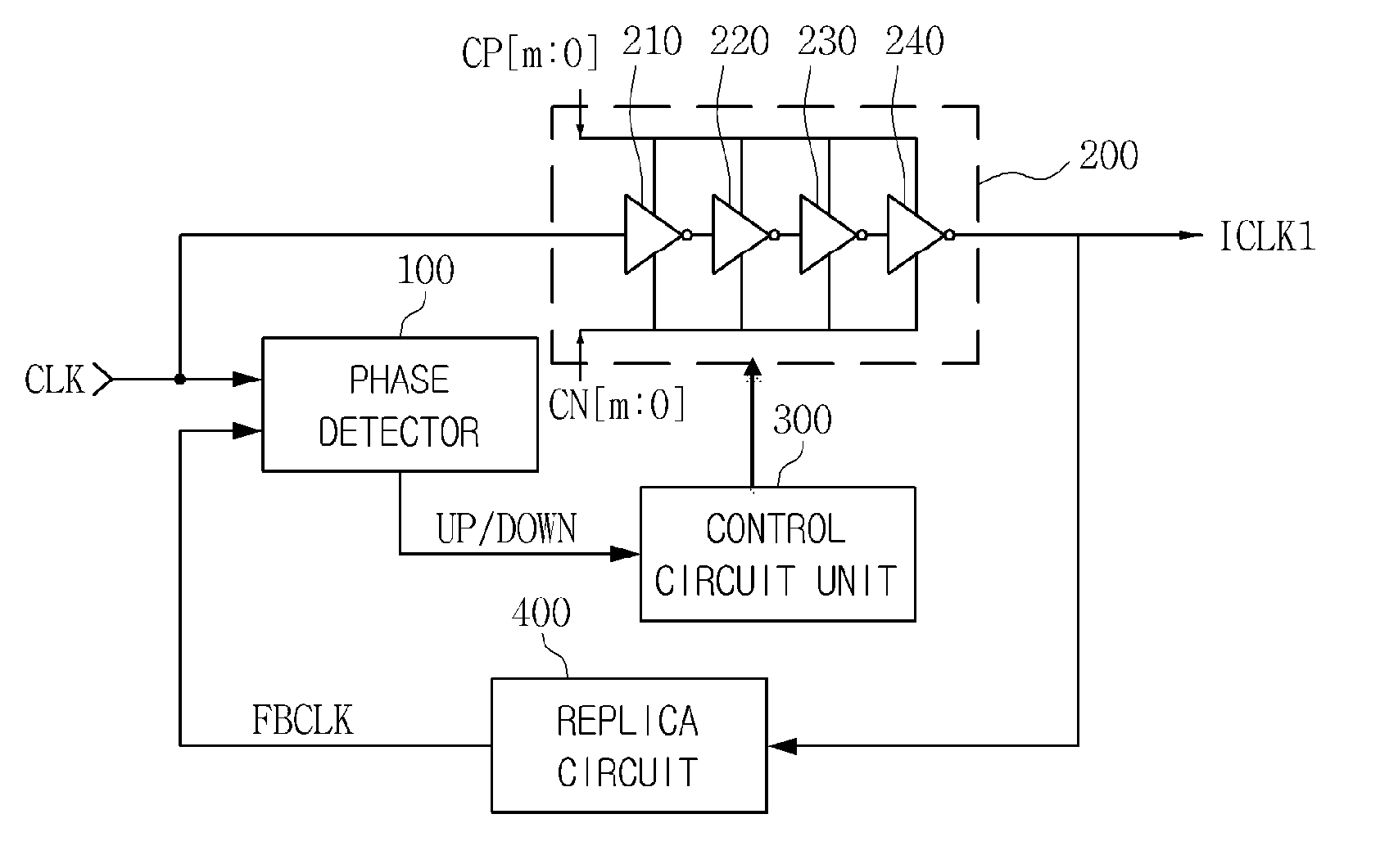
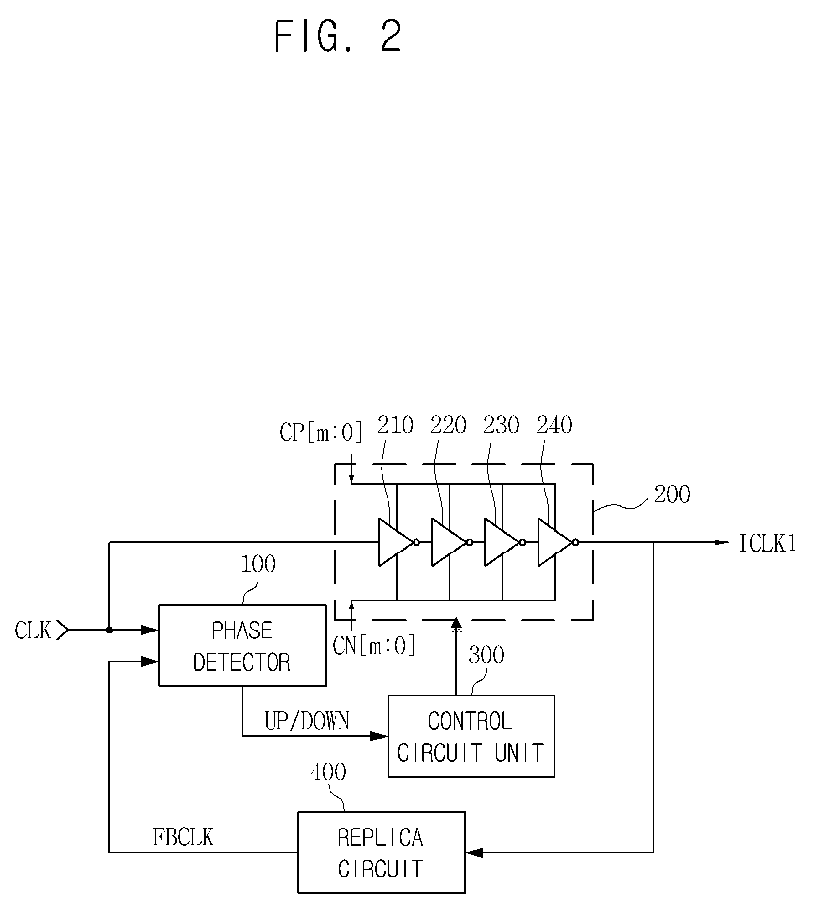
[0025]Example embodiments will now be described more fully hereinafter with reference to the accompanying drawings. Exemplary embodiments may, however, be embodied in different forms and should not be construed as limited to the embodiments set forth herein.

[0026]It will be understood that when an element is referred to as being “connected” or “coupled” to another element, it can be directly connected or coupled to the other element or intervening elements may be present. In contrast, when an element is referred to as being “directly connected” or “directly coupled” to another element, there are no intervening elements present. As used herein the term “and / or” includes any and all combinations of one or more of the associated listed items.

[0027]It will be understood that, although the terms “first”, “second”, etc., may be used herein to describe various elements, components, regions, and / or sections, these elements, components, regions, and / or sections should not be limited by these...


PUM


Abstract

A delay locked loop circuit is disclosed. The circuit includes a phase detector for comparing the phase of an input clock signal with the phase of a feedback clock signal that is fed back into the phase detector, and for outputting a detection signal. The circuit also includes a control circuit unit for controlling a delay line in response to the detection signal, a delay line for delaying the input clock by a predetermined amount of delay in response to output impedance calibration codes applied to the delay line, and a replica circuit configured to have the same delay conditions as those of an actual clock path to a circuit of the semiconductor device, to receive a delay clock signal of the delay line, and to generate the feedback clock signal.

Description

CROSS-REFERENCE TO RELATED APPLICATIONS[0001]This application claims the benefit of Korean Patent Application No. 10-2009-0018438, filed on Mar. 4, 2009, in the Korean Intellectual Property Office, and entitled: “Delay Locked Loop Circuit Including Delay Line Insensitive to Variation in PVT,” the contents of which are incorporated by reference herein in their entirety.BACKGROUND[0002]1. Field[0003]The embodiments disclosed herein relate to a delay locked loop circuit, and more particularly, to a delay locked loop circuit including a delay line capable of delaying an input clock signal by a predetermined amount of delay so as to reduce sensitivity to variations in PVT (process, voltage, and / or temperature), and a synchronous semiconductor memory device including the same.[0004]2. Description of the Related Art[0005]In recent years, the speed and the degree of integration of dynamic random access memories generally used as the main memories of electronic systems have increased in orde...

Claims


Application Information

Patent Timeline
Patent Type & Authority Patents(United States)
IPC IPC(8): G11C7/00
CPCG11C7/04G11C7/22G11C7/222G11C11/4076G11C29/02G11C29/023G11C29/028G11C8/00G11C11/407H03L7/08
Inventor CHOI, SEOK-WOO
Owner SAMSUNG ELECTRONICS CO LTD
Why Eureka
Try Eureka