Integrated circuits on a wafer and method for separating integrated circuits on a wafer

a technology of integrated circuits and wafers, which is applied in the direction of electrical equipment, semiconductor devices, semiconductor/solid-state device details, etc., can solve the problems of missing saw lines, milky appearance, and inability to distinguish integrated circuits from saw lines, so as to achieve the effect of more reliable separation of integrated circuits formed thereon

Active Publication Date: 2013-04-09
NXP BV
View PDF8 Cites 1 Cited by
  • Summary
  • Abstract
  • Description
  • Claims
  • Application Information

AI Technical Summary

Benefits of technology

[0004]It is an object of the present invention to provide a wafer which allows separating the integrated circuits formed thereon more reliably particularly when utilizing the bottom surface of the wafer.
[0009]The inventive integrated circuits on the wafer comprise the wafer substrate and the integrated circuits formed on the surface of the wafer substrate. The integrated circuits are formed on the wafer substrate by depositing the plurality of superposed layers on this wafer surface and by depositing the top layer on the superposed layers. The top layer may particularly be a passivation layer. A passivation layer is a sealing layer added, for instance, at the end of the fabrication process of the integrated circuits on the wafer to prevent deterioration of electronic properties through, for instance, chemical action, corrosion, or handling during a packaging process. The passivation layer may be comprised of silicon dioxide or silicon nitride, and may protect against moisture or contamination.
[0013]The at least one layer of the superposed layers forming the alignment marks may particularly be a metallization layer. This metallization layer may comprise TiW, Al, or Cu. The term “metallization layer” shall not only denote a pure metal, but shall also include metal alloys. The internal alignment marks made from metal allows light which shines onto the bottom surface of the wafer substrate to be reflected and thus allows automatic detection of the alignment mark. The detected alignment marks are then utilized for aligning the separating device.
[0015]The superposed layers may be comprised of a plurality of superposed metallization layers, of which at least the metallization layer located next to the wafer substrate forms the alignment marks. This reduces the amount of light to be absorbed by the wafer substrate before being reflected by the alignment marks, potentially improving automatic detection of the alignment marks.
[0016]If the superposed layers are comprised of the plurality of superposed metallization layers, then some or all of the metallization layers may form the alignment marks. The metallization layers may be relatively thin and thus only reflect a part of the light shining through the bottom surface of the wafer substrate and reaching the metallization layer. Utilizing some or even all of the metallization layers for the alignment marks increases the amount of potentially reflected light, potentially improving automatic alignment.
[0018]The areas surrounding the actual alignment marks may be comprised of an N-well formed into the surface of the wafer substrate, a P-type layer applied on the N-well, and at least one metallization layer applied on the P-type layer. The areas surrounding the actual alignment marks may be comprised of a P-well formed into the surface of the wafer substrate, an N-type layer applied on the P-well, and at least one metallization layer applied on the N-type layer. Such a structure may relatively well absorb light shining through the bottom surface of the wafer substrate and thus improves the contrast of the alignment marks.

Problems solved by technology

Particularly, when utilizing the bottom surface of the wafer for separating the integrated circuits, then the structure of the integrated circuits may not be detected reliably, potentially resulting in not distinguishing the saw lines from the integrated circuits and, thus, potentially missing the saw lines.
This may even more pronounced if the saw lines are relatively narrow, virtually zero when utilizing laser-dicing, or almost zero when utilizing trench etching, or if the wafer comprises an epitaxial wafer substrate resulting in a milky appearance.

Method used


Image

  • Integrated circuits on a wafer and method for separating integrated circuits on a wafer
  • Integrated circuits on a wafer and method for separating integrated circuits on a wafer
  • Integrated circuits on a wafer and method for separating integrated circuits on a wafer

Examples


Embodiment Construction

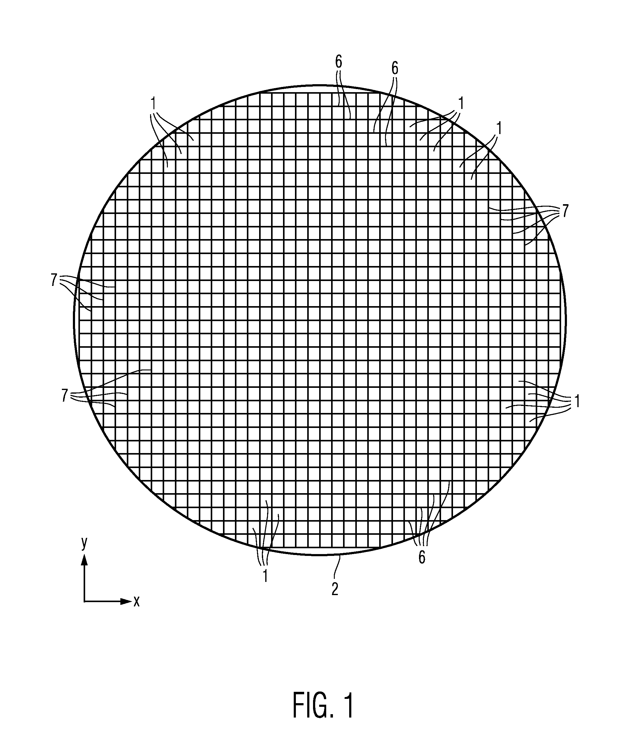
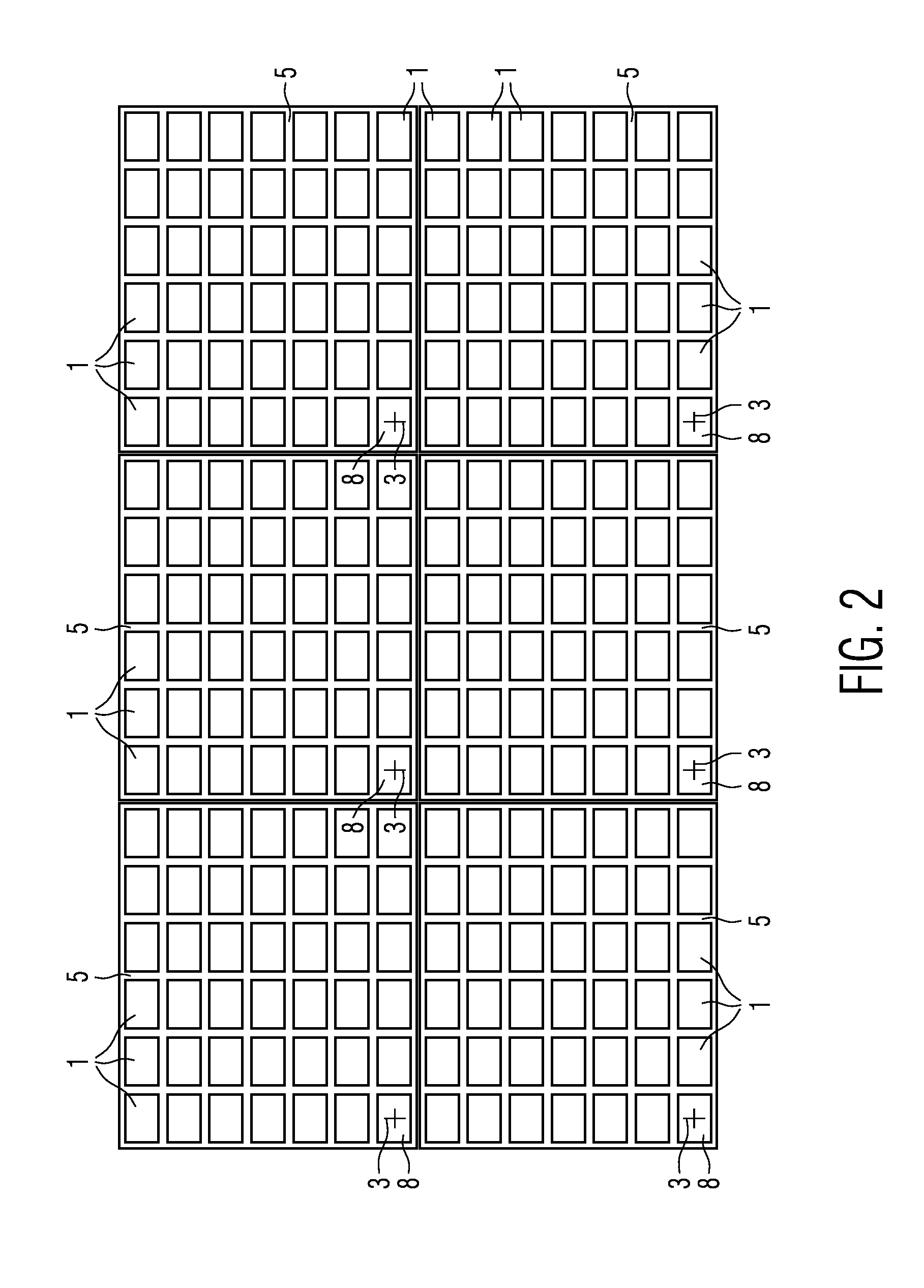
[0037]FIG. 1 shows a top-view of a plurality of integrated circuits 1 on a semiconductor wafer and FIG. 2 shows a part of this top-view.

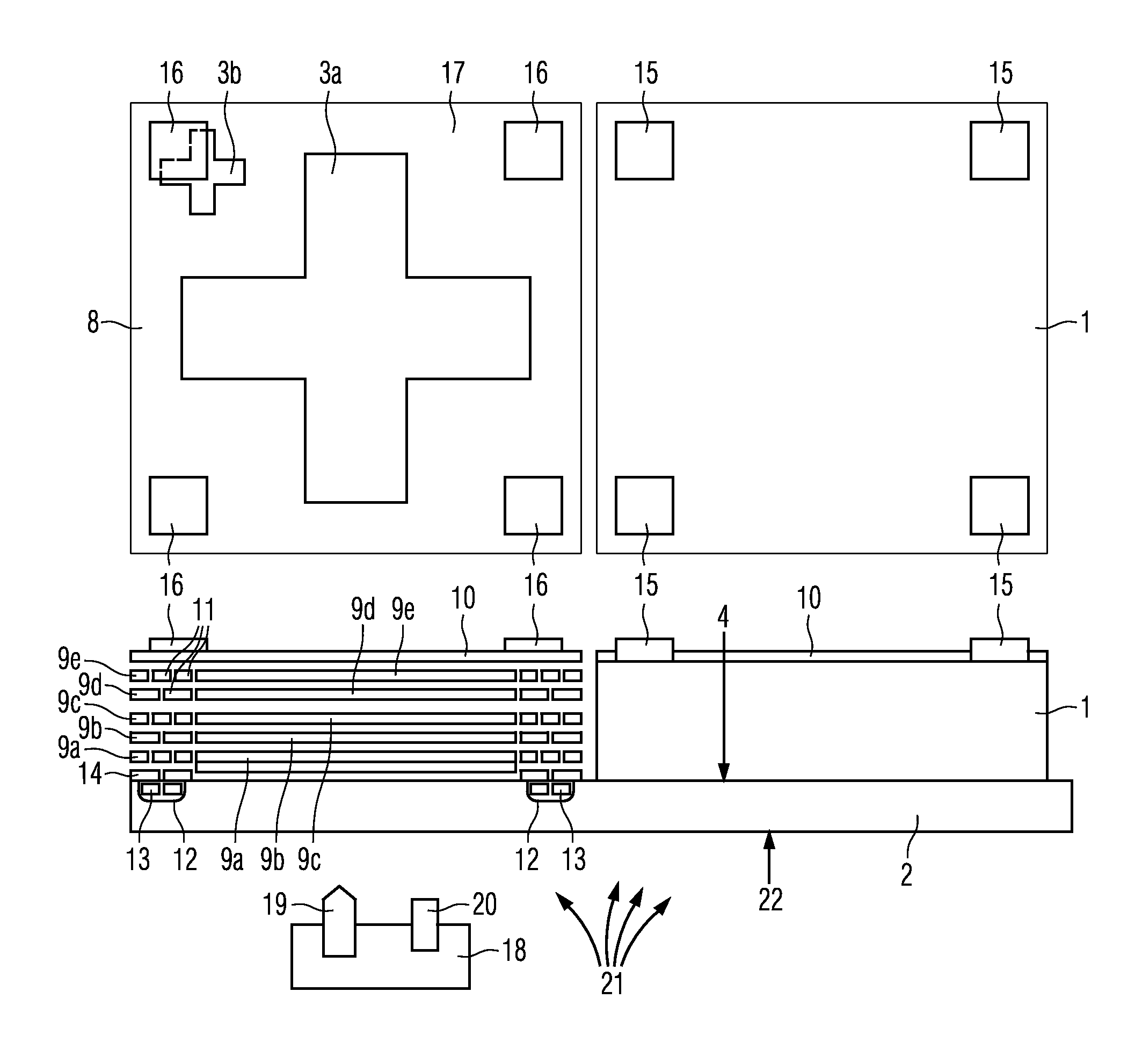
[0038]The integrated circuits 1 have been formed on a wafer substrate 2 as it is generally known per se in the art by forming a plurality of layers on the wafer substrate 2. For the exemplary embodiment, not only the integrated circuits 1 are formed on the wafer substrate 2, but also alignment marks 3. A top view and a cross section of one of the alignment marks 3 are shown in FIG. 3. The alignment marks 3 are utilized for aligning a separating device 18 used during a separation step during which the integrated circuits 1 on the wafer are separated into individual integrated circuits 1.

[0039]For the exemplary embodiment, the integrated circuits 1 and the alignment marks 3 have been formed on an upper wafer surface 4 of the wafer substrate 2 utilizing a reticle. When manufacturing the integrated circuits 1 on the wafer utilizing a reticle, an area of...


PUM


Abstract

Integrated circuits (1) on a wafer comprise a wafer substrate (2) and a structure applied on a surface (4) of the wafer substrate (2). The structure forms a plurality of integrated circuits (1) formed on the wafer substrate (2) and the integrated circuits (1) are separated by saw lines (6, 7). The structure comprises a plurality of superposed layers (9a-9e) formed on the wafer substrate (2) and a top layer (10) formed on the superposed layers (9a-9e). The integrated circuit (1) on the wafer further comprise a plurality of alignment marks (3) intended for aligning a separating device (18) for separating the integrated circuits (1) on the wafer into individual integrated circuits (1) during a separation process, wherein the alignment marks (3) are formed from at least one of the superposed layers (9a-9e).

Description

FIELD OF THE INVENTION[0001]The invention relates to integrated circuits on a wafer and to a method for separating integrated circuits on a wafer.BACKGROUND OF THE INVENTION[0002]Integrated circuits are usually produced by forming a plurality of integrated circuits on a semiconductor wafer substrate. The individual integrated circuits are separated by saw lines. The finished integrated circuits on the wafer are then separated into individual integrated circuits by, for instance, sawing the wafer along the saw lines or utilizing a scribe method. When separating the individual integrated circuits, a saw or a laser may be guided along the saw lines. In order to target the saw lines, the saw or laser may be aligned utilizing the pattern defined by the integrated circuits on the wafer.[0003]The saw or laser may be guided on the top surface of the wafer, i.e. the surface of the wafer substrate on which the integrated circuits are formed, or may be guided on the bottom surface of the wafer...

Claims


Application Information

Patent Timeline
Patent Type & Authority Patents(United States)
IPC IPC(8): H01L23/544H01L21/78
CPCH01L23/544H01L2223/5442H01L2223/54426H01L2223/54466H01L2924/0002H01L2223/5448H01L2924/00
Inventor SCHEUCHER, HEIMOALBERMANN, GUIDOCECCARELLI, DAVID
Owner NXP BV
Why Eureka
Try Eureka